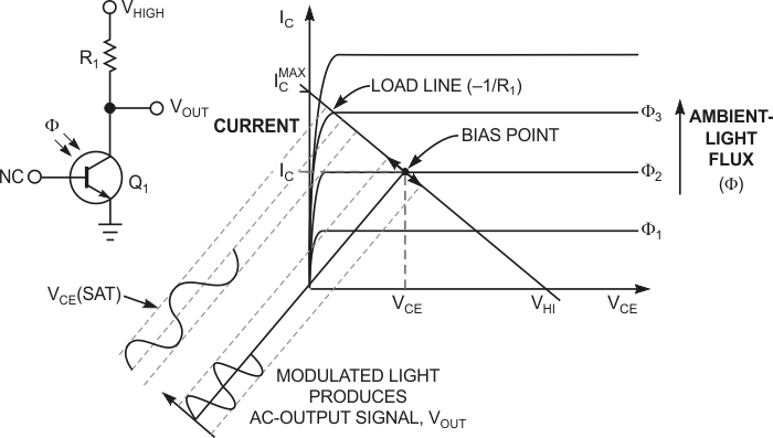
A designer who uses a phototransistor to convert a modulated optical signal to an electrical signal frequently encounters problems when high-intensity background light saturates the phototransistor. When its base terminal floats, a phototransistor's collector-to-emitter voltage depends only on the photocurrent generated by the superposition of the signal and background light. The phototransistor's gain and its active-region range depend on R1’s resistance. For higher values of R1, the circuit's gain increases, but the phototransistor saturates more quickly. In Figure 1, without background illumination, the transistor operates in its linear region at bias point Φ2, and Q1’s collector voltage varies linearly around VCE. Its output, VOUT, faithfully reproduces amplitude fluctuations in the modulated optical signal. Applying extraneous steady-state background illumination shifts the circuit's operating point to bias point Φ3, and the output voltage compresses and distorts.
 |
||
| Figure 1. | Varying levels of ambient-light flux affect the bias point of a basic phototransistor circuit. Higher levels force the bias point closer to saturation and compress the desired signal, VOUT. |
|
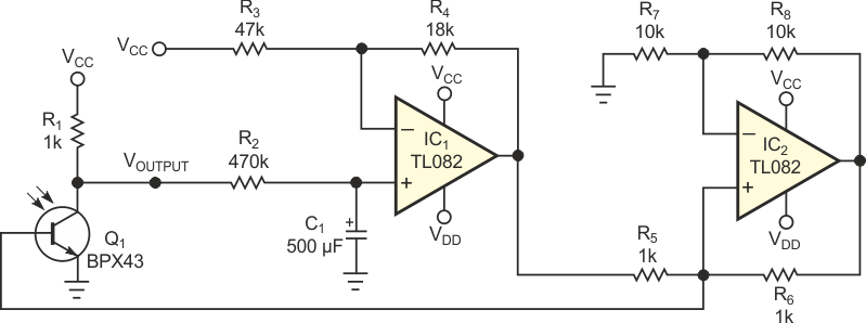
Unlike photodiodes and photovoltaic cells that have only two leads, a phototransistor's base connection allows a feedback circuit to control the device's bias point. Diverting current from the base terminal reduces collector current. In Figure 2, phototransistor Q1 detects an optical signal plus background light that illuminates its base region. A lowpass active filter samples the collector voltage generated by the background light, and a Howland current source alters the circuit's bias point by draining current from the phototransistor's reverse-biased collector-base junction.
 |
||
| Figure 2. | A feedback circuit consisting of a single-pole lowpass active filter and a Howland source diverts current from the phototransistor’s base to avoid saturation at excessive background-light levels. |
|
In general, extraneous background illumination fluctuates more slowly than the desired signal. For simplicity, this design uses a first-order lowpass filter, C1 and R2, with a cutoff frequency below the signal frequency to sample Q1’s collector voltage. Applying a reference voltage – VCC, in this example – to R3 sets the filter circuit's dc operating point midway between the phototransistor's cutoff and saturation voltages. The lowpass filter's output drives a Howland current source to produce a current proportional to the filter's output. As background illumination increases, Q1’s collector voltage decreases. The current source's output subtracts from Q1’s base current, which in turn raises Q1’s collector voltage to avoid saturation.
The ratio of R4 to R3 establishes the active lowpass filter's gain according to the equation
and R5 sets the current source's transconductance:
Altering these resistors affects the amount of current drained from the phototransistor's base and the circuit's operating point. The phototransistor has much lower capacitance than the filter, ensuring that the circuit in Figure 2 cannot oscillate. However, replacing the first-order lowpass filter with a second-order lowpass filter requires careful selection of the capacitors' values to avoid oscillation.
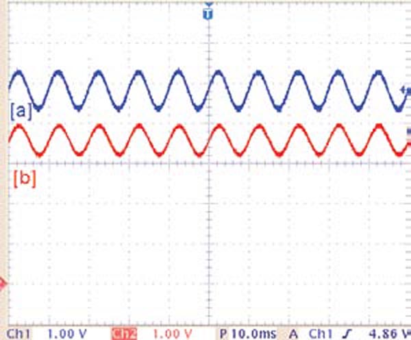
Illuminating the phototransistor with a 100 W incandescent light bulb provides high-intensity-light background lighting plus a rapidly changing signal due to the applied ac-line voltage. Figure 3 shows Q1’s collector-to-emitter voltage with the light bulb 40 cm from the phototransistor with the feedback circuit active (Figure 3a) and for the circuit with the phototransistor's base floating (Figure 3b). The responses appear similar because the phototransistor doesn't saturate at the applied light intensity.
 |
||
| Figure 3. | A 100 W light bulb at a 40-cm distance illuminates a collector-emitter voltage of a phototransistor with a feedback circuit (a) and with no feedback (b). Both bias points remain in the linear region. |
|
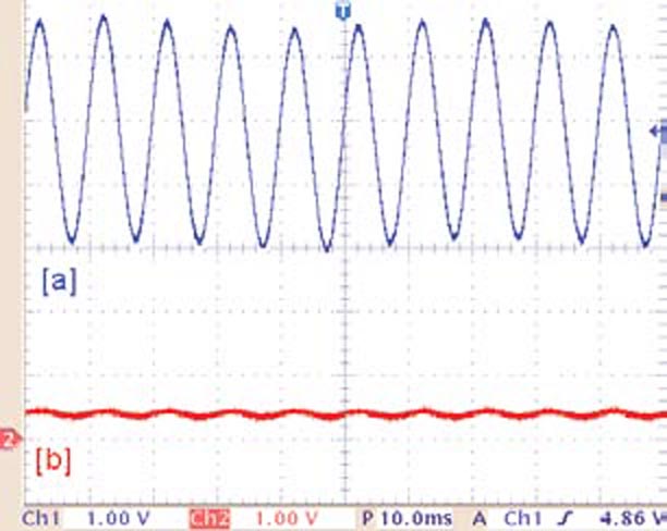
Repositioning the light bulb at 20 cm from the phototransistor increases the background-light level and drives the phototransistor closer to saturation. When you apply feedback, the phototransistor delivers a higher amplitude signal, although its bias point remains almost unchanged (Figure 4a). The average dc-voltage level at Q1’s collector remains almost the same as at the lower light level (Figure 3a). However, with no feedback applied, the phototransistor's bias point moves close to saturation, and the ac-modulated light variations are barely detectable (Figure 4b).
 |
||
| Figure 4. | A 100 W light bulb at a 20-cm distance illuminates the collector-emitter voltage of a phototransistor with a feedback circuit (a) and with no feedback (b). Saturation of the circuit with no feedback prevents signal detection. |
|