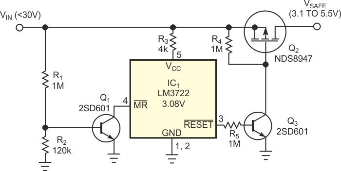
Supervisory circuits normally monitor a microprocessor's supply voltage, asserting reset to the IC during power-up, power-down, and brownout. In this way, the circuit ensures that the supply voltage is stable before the microprocessor boots, thus preventing code-execution errors. Many analog and digital ICs also need a well-behaved start-up of their supply to avoid latch-up and logic-state errors. In addition to low-supply conditions, low-voltage CMOS circuits need overvoltage protection from any supply runaway. The additional components in Figure 1 extend IC1’s supervisory functions to connect VIN to VSAFE only when VIN is within set limits. This function protects circuitry at the VSAFE terminal from power-up transients and overvoltage damage. As a supervisory circuit, IC1 asserts a reset signal that is delayed by more than 100 msec whenever VIN decreases below the precisely trimmed reset threshold. You can custom-select the reset threshold from 2.32 to 4.63 V. You can also use a manual input, /MR, to assert the reset signal.
 |
||
| Figure 1. | This LM3722 configuration connects only safe voltages to sensitive ICs. | |
This application uses IC1’s delayed reset signal to control switch Q2. The delay ensures that VIN is stable before application to VSAFE. Q3 inverts and isolates IC1’s reset signal to control the gate of Q2. R4 is Q2’s pullup resistor; R5 limits Q3’s base current. Using Q1 as an inexpensive 0.6 V switch, resistor dividers R1 and R2 set the overvoltage threshold according to the equation
| Table 1. | VSAFE hysteresis over temperature | |||||||||||||||||||||||||
|
||||||||||||||||||||||||||
An internal 22-kΩ resistor at IC1’s /MR input provides Q2’s pullup. Typical VBE1 accuracy and temperature-coefficient errors are ±10% and –2 mV/°C, respectively. Adjustment of R2 for an exact overvoltage value nullifies VBE1’s accuracy error. Table 1 shows typical setpoints over temperature. If you need further error reduction, you could exchange Q2 for a comparator and voltage reference. For VIN within the set limits, 3.1 to 5.5 V, the circuit draws only 16 µA. A total of 5 µA flows into both the R1 and R4 nodes, and 6 µA flows into R3’s node. R3 protects IC1 by providing current limiting of less than 6 mA) for high voltages at VIN. The typical IC1 current of 6 µA through R3 increases the undervoltage setpoint by 24 mV.