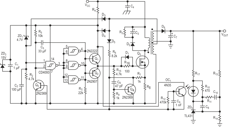
Figure 1 shows a flyback power supply that has low noise and uses a simple CMOS CD4093 IC for its control. The electrical noise of a converter arises mainly when current switches on. Diode recovery and charging parasitic capacitances create high di/dt, which is the main cause of noise. The converter in Figure 1 has a low noise level, because it slowly switches current on at nearly zero voltage. The converter works in the boundary between discontinuous and continuous mode and switches on when the drain voltage is at its lowest value. To avoid working with low gate voltages, which would cause excessive MOSFET losses, ZD1 conducts and enables the input gate of the CD4093 when the voltage is high enough. When the supply starts, the auxiliary nonisolated winding through D3 keeps the gate input high. When the MOSFET is on, current increases linearly until the base of Q5 starts to conduct, and this transistor turns the MOSFET off. The flyback operation then starts, and the primary energy charges the output capacitors. During this phase of operation, D5 and R6 keep Q5 conducting and the MOSFET off. When the energy has discharged, D5 stops conducting, as do the secondary diodes, so no recovery problems exist.
 |
||
| Figure 1. | Using a simple CMOS IC, this flyback power-supply circuit exhibits extremely low noise. | |
The time constant of R5 and C5 keeps the MOSFET off for a while. The output capacitance of the MOSFET plus the parasitic capacitance of the primary resonate with the primary inductance and the voltage decreases. R5 and C5 allow the MOSFET to turn on when the voltage has reached the minimum value. The values are valid only for this case. The circuit of Figure 1 not only minimizes turn-on losses, but also reduces electrical noise. Voltage regulation uses traditional techniques, using a TL431. The optocoupler current adds to the shunt current. Because the MOSFET turns on when current is zero, the gate resistor may be high, so parasitic capacitances charge slowly, further reducing switching noise. The circuit around Q4 is optional; you can use it in most power supplies. It kills the current glitch when Q3 turns on. It is more effective than the usual RC circuit, and it allows a low duty cycle at low loads. Note that many of the component values in Figure 1 are undesignated; you should determine these values to fit the application.