Amplifiers with positive feedback are the bases of signal-grade pulse-forming circuits. This setup ensures a triggerlike operation in which the input signal crosses the input-threshold level; in most cases, the input signal is a voltage signal. The most well-known of these triggers is the Schmitt trigger, which recently celebrated its 80th birthday. American scientist OH Schmitt in 1938 originated the Schmitt trigger in the form of a two-stage amplifier with current feedback. The two active devices were vacuum tubes.
The operation of a Schmitt trigger has the advantage of fast, almost-constant transition times of the output regardless of the slope of the input signal. One consequence of this type of operation is the hysteresis in the I/O characteristic. In other words, the threshold shifts to a higher value before the positive-output transition, and it shifts to a lower value after switching to the positive-output level. You can set the amount of hysteresis – from zero to latch-up – for Schmitt-trigger circuits comprising discrete parts. Schmitt circuits find wide use in logic ICs, in which the hysteresis is rather high and fixed.
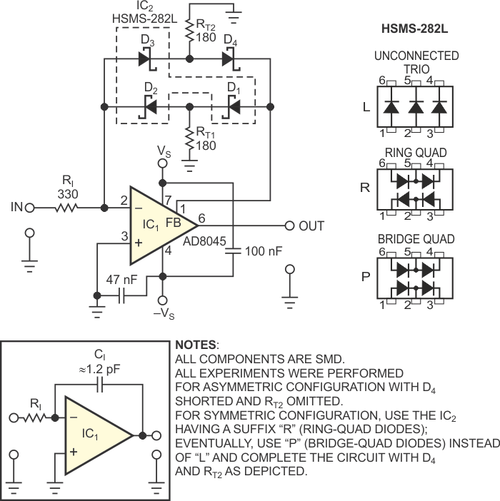
As an alternative, you can use a circuit – a fast-response voltage limiter, or clamper – as a pulse-forming circuit. The input-voltage range is narrower than that of Schmitt-trigger circuits, because, at low input voltages, the voltage limitation becomes inactive, and the circuit operates as a linear amplifier. On the other hand, because of its nonhysteretic behavior, the decision threshold of the input voltage is precise and equal for both directions of output-level transitions. Figure 1 shows one example of such as circuit. The voltage limiter in Figure 1 is an inverting amplifier with a highly nonlinear negative feedback. For output voltages ranging from –0.3 to +0.6 V, the feedback impedance is high because each of the diodes is nonconducting. The forward-voltage drop of the selected Schottky-barrier diodes determines these voltage limits. The voltage gain of the inverting amplifier is thus almost that of the op amp’s open-loop gain.
 |
||
| Figure 1. | This clamping circuit uses diodes to achieve nonlinear feedback. The circuit employs a single diode in one feedback path and two diodes in the other. The dual-diode configuration offers cleaner switching. |
|
Whenever the output voltage exceeds these limits, diode D1, D2, or D3 – depending on the polarity of the output voltage – starts to conduct. The differential gain of the amplifier then drops to the value of –RI/2RD and –RI/RD, respectively, where RD is the equivalent-series resistance of a single diode. The action clamps the output voltage to approximately 0.8 V and to –0.4 V even for large input voltages. The figure uses an Analog Devices AD8045 VHSIC (very-high-speed integrated-circuit) op amp because its slew rate exceeds the value of 1 V/nsec.
Figure 1’s circuit has an asymmetrical-limiting configuration to compare the single feedback diode with two series-connected diodes having a transverse resistor, RT1, between their midpoints and ground. The clamping circuitry comprising D1, D2, and RT1 offers higher off-isolation between the output and the input of the op amp than that of the single diode, D3. When D3 is on, you can observe small, weakly damped oscillations at approximately 200 MHz in the output waveform. Oscillations manifest themselves less at the beginning of turn-on of the D1 and D2 diodes.