Despite its critical nature in high-speed circuitry, printed-circuit-board (PCB) layout is often one of the last steps in the design process. There are many aspects to high-speed PCB layout; volumes have been written on the subject. This article addresses high-speed layout from a practical perspective. A major aim is to help sensitize newcomers to the many and various considerations they need to address when designing board layouts for high-speed circuitry. But it is also intended as a refresher to benefit those who have been away from board layout for a while. Not every topic can be covered in detail in the space available here, but we address key areas that can have the greatest payoff in improving circuit performance, reducing design time, and minimizing time-consuming revisions.
Although the focus is on circuits involving high-speed op amps, the topics and techniques discussed here are generally applicable to layout of most other high-speed analog circuits. When op amps operate at high RF frequencies, circuit performance is heavily dependent on the board layout. A high-performance circuit design that looks good "on paper" can render mediocre performance when hampered by a careless or sloppy layout. Thinking ahead and paying attention to salient details throughout the layout process will help ensure that the circuit performs as expected.
The Schematic
Although there is no guarantee, a good layout starts with a good schematic. Be thoughtful and generous when drawing a schematic, and think about signal flow through the circuit. A schematic that has a natural and steady flow from left to right will tend to have a good flow on the board as well. Put as much useful information on the schematic as possible. The designers, technicians, and engineers who will work on this job will be most appreciative, including us; at times we are asked by customers to help with a circuit because the designer is no longer there.
What kind of information belongs on a schematic besides the usual reference designators, power dissipations, and tolerances? Here are a few suggestions that can turn an ordinary schematic into a superschematic! Add waveforms, mechanical information about the housing or enclosure, trace lengths, keep-out areas; designate which components need to be on top of the board; include tuning information, component value ranges, thermal information, controlled impedance lines, notes, brief circuit operating descriptions … (and the list goes on).
Trust No One
If you're not doing your own layout, be sure to set aside ample time to go through the design with the layout person. An ounce of prevention at this point is worth more than a pound of cure! Don't expect the layout person to be able to read your mind. Your inputs and guidance are most critical at the beginning of the layout process. The more information you can provide, and the more involved you are throughout the layout process, the better the board will turn out. Give the designer interim completion points - at which you want to be notified of the layout progress for a quick review. This "loop closure" prevents a layout from going too far astray and will minimize reworking the board layout.
Your instructions for the designer should include:
- a brief description of the circuit's functions;
- a sketch of the board that shows the input and output locations;
- the board stack up (i.e., how thick the board will be, how many layers, details of signal layers and planes - power, ground, analog, digital, and RF);
- which signals need to be on each layer;
- where the critical components need to be located;
- the exact location of bypassing components;
- which traces are critical;
- which lines need to be controlled-impedance lines;
- which lines need to have matched lengths; component sizes;
- which traces need to kept away from (or near) each other;
- which circuits need to be kept away from (or near) each other;
- which components need to be close to (or away from) each other;
- which components go on the top and the bottom of the board.
You'll never get a complaint for giving someone too much information - too little, yes; too much, no.
A learning experience: About 10 years ago I designed a multilayer surface-mounted board - with components on both sides of the board. The board was screwed into a gold-plated aluminum housing with many screws (because of a stringent vibration spec). Bias feed-through pins poked up through the board. The pins were wire-bonded to the PCB. It was a complicated assembly. Some of the components on the board were to be SAT (set at test). But I hadn't specified where these components should be. Can you guess where some of them were placed? Right! On the bottom of the board. The production engineers and technicians were not very happy when they had to tear the assembly apart, set the values, and then reassemble everything. I didn't make that mistake again.
Location, Location, Location
As in real estate, location is everything. Where a circuit is placed on a board, where the individual circuit components are located, and what other circuits are in the neighborhood are all critical.
Typically, input-, output-, and power locations are defined, but what goes on between them is "up for grabs." This is where paying attention to the layout details will yield significant returns. Start with critical component placement, in terms of both individual circuits and the entire board. Specifying the critical component locations and signal routing paths from the beginning helps ensure that the design will work the way it's intended to. Getting it right the first time lowers cost and stress - and reduces cycle time.
Power-Supply Bypassing
Bypassing the power supply at the amplifier's supply terminals to minimize noise is a critical aspect of the PCB design process - both for high-speed op amps and any other high-speed circuitry. There are two commonly used configurations for bypassing high-speed op amps.
Rails to ground: This technique, which works best in most cases, uses multiple parallel capacitors connected from the op amp's power-supply pins directly to ground. Typically, two parallel capacitors are sufficient - but some circuits may benefit from additional capacitors in parallel.
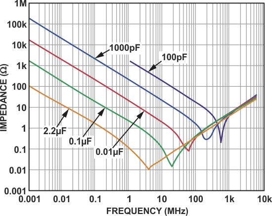
Paralleling different capacitor values helps ensure that the power supply pins see a low ac impedance across a wide band of frequencies. This is especially important at frequencies where the op-amp power-supply rejection (PSR) is rolling off. The capacitors help compensate for the amplifier's decreasing PSR. Maintaining a low impedance path to ground for many decades of frequency will help ensure that unwanted noise doesn't find its way into the op amp. Figure 1 shows the benefits of multiple parallel capacitors. At lower frequencies the larger capacitors offer a low impedance path to ground. Once those capacitors reach self resonance, the capacitive quality diminishes and the capacitors become inductive. That is why it is important to use multiple capacitors: when one capacitor's frequency response is rolling off, another is becoming significant, thereby maintaining a low ac impedance over many decades of frequency.
 |
||
| Figure 1. | Capacitor impedance vs. frequency. | |
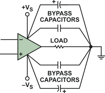
Starting directly at the op amp's power-supply pins; the capacitor with the lowest value and smallest physical size should be placed on the same side of the board as the op amp - and as close to the amplifier as possible. The ground side of the capacitor should be connected into the ground plane with minimal lead- or trace length. This ground connection should be as close as possible to the amplifier's load to minimize disturbances between the rails and ground. Figure 2 illustrates this technique.
 |
||
| Figure 2. | Parallel-capacitor rails-to-ground bypassing. | |
This process should be repeated for the next-higher-value capacitor. A good place to start is with 0.01 µF for the smallest value, and a 2.2-µF - or larger - electrolytic with low ESR for the next capacitor. The 0.01 µF in the 0508 case size offers low series inductance and excellent high-frequency performance.
Rail to rail: An alternate configuration uses one or more bypass capacitors tied between the positive- and negative supply rails of the op amp. This method is typically used when it is difficult to get all four capacitors in the circuit. A drawback to this approach is that the capacitor case size can become larger, because the voltage across the capacitor is double that of the single-supply bypassing method. The higher voltage requires a higher breakdown rating, which translates into a larger case size. This option can, however, offer improvements to both PSR and distortion performance.
Since each circuit and layout is different; the configuration, number, and values of the capacitors are determined by the actual circuit requirements.
Parasitics
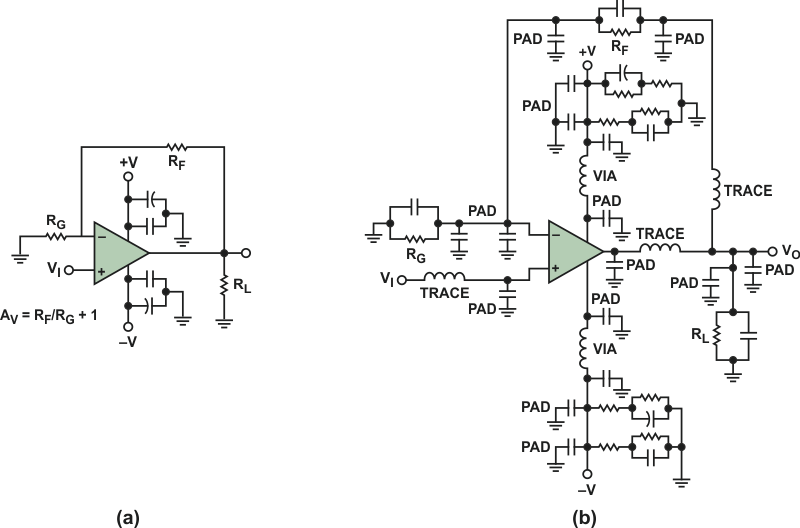
Parasitics are those nasty little gremlins that creep into your PCB (quite literally) and wreak havoc within your circuit. They are the hidden stray capacitors and inductors that infiltrate high-speed circuits. They include inductors formed by package leads and excess trace lengths; pad-to-ground, pad-to-power-plane, and pad-to-trace capacitors; interactions with vias, and many more possibilities. Figure 3(a) is a typical schematic of a noninverting op amp. If parasitic elements were to be taken into account, however, the same circuit would look like Figure 3(b).
 |
||
| Figure 3. | Typical op amp circuit, as designed (a) and with parasitics (b). | |
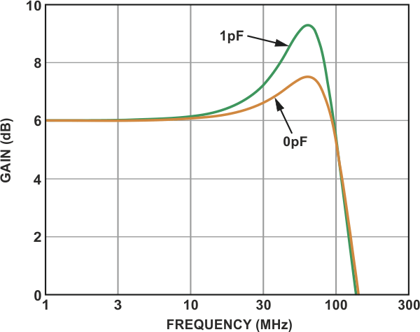
In high-speed circuits, it doesn't take much to influence circuit performance. Sometimes just a few tenths of a picofarad is enough. Case in point: if only 1 pF of additional stray parasitic capacitance is present at the inverting input, it can cause almost 2 dB of peaking in the frequency domain (Figure 4). If enough capacitance is present, it can cause instability and oscillations.
 |
||
| Figure 4. | Additional peaking caused by parasitic capacitance. | |
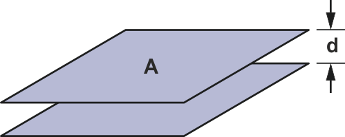
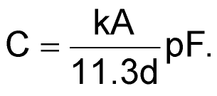
A few basic formulas for calculating the size of those gremlins can come in handy when seeking the sources of the problematic parasitics. Equation 1 is the formula for a parallel-plate capacitor (see Figure 5).
 |
||
| Figure 5. | Capacitance between two plates. | |
 |
(1) |
C is the capacitance, A is the area of the plate in cm2, k is the relative dielectric constant of board material, and d is the distance between the plates in centimeters.
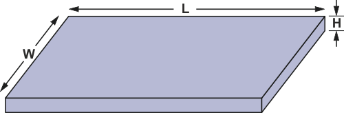
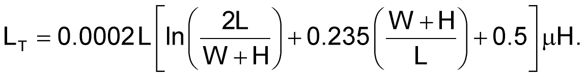
Strip inductance is another parasitic to be considered, resulting from excessive trace length and lack of ground plane. Equation 2 shows the formula for trace inductance. See Figure 6.
 |
||
| Figure 6. | Inductance of a trace length. | |
 |
(2) |
W is the trace width, L is the trace length, and H is the thickness of the trace. All dimensions are in millimeters.
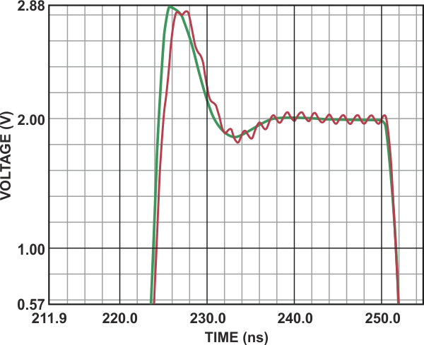
The oscillation in Figure 7 shows the effect of a 2.54-cm trace length at the noninverting input of a high-speed op amp. The equivalent stray inductance is 29 nH (nanohenry), enough to cause a sustained low-level oscillation that persists throughout the period of the transient response. The picture also shows how using a ground plane mitigates the effects of stray inductance.
 |
||
| Figure 7. | Pulse response with - and without - ground plane. | |
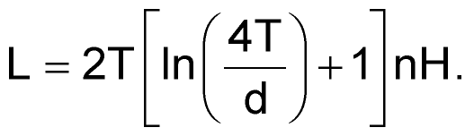
Vias are another source of parasitics; they can introduce both inductance and capacitance. Equation 3 is the formula for parasitic inductance (see Figure 8).
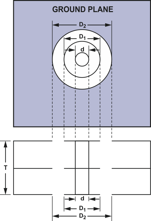 |
||
| Figure 8. | Via dimensions. | |
 |
(3) |
T is the thickness of the board and d is the diameter of the via in centimeters.
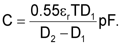
Equation 4 shows how to calculate the parasitic capacitance of a via (see Figure 8).
 |
(4) |
εr is the relative permeability of the board material. T is the thickness of the board. D1 is the diameter of the pad surrounding the via. D2 is the diameter of the clearance hole in the ground plane. All dimensions are in centimeters. A single via in a 0.157-cm-thick board can add 1.2 nH of inductance and 0.5 pF of capacitance; this is why, when laying out boards, a constant vigil must be kept to minimize the infiltration of parasites!