Care must be exercised when you try to “quickly” charge a nickel-cadmium (NiCd) cell or battery pack at a current density that approaches or exceeds one-third of its capacity (C/3). As the battery becomes fully charged, the high charging current raises both the internal cell pressure and temperature, which can quickly degrade the battery or destroy it.
One way to avoid damage is to monitor the differential temperature (TDIFF) between the battery’s surface temperature (TB) and the ambient (TA) and to proportionally reduce the charging current (ICH) as the differential temperature increases. Of course, you must make sure that the sensor monitoring the ambient environment is attached to a structure that approximates the thermal mass of the battery pack. Otherwise, the resulting difference in thermal delays will adversely affect results.
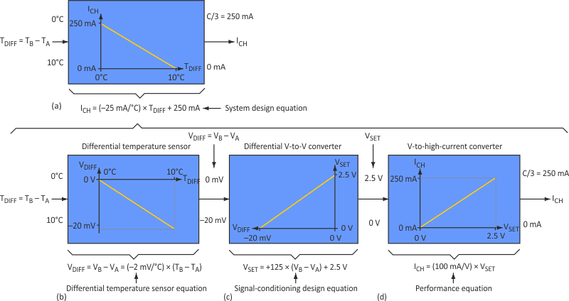
Consider an example design that must convert a differential temperature ranging from 0 °C to 10 °C into a charging current that decreases proportionally from C/3 to 0 A. If C equals 750 mA, C/3 equals 250 mA and the equation to describe this linear system is:
 |
(1) |
Figure 1 represents this design equation (Fig. 1a), including graphical and mathematical descriptions of the main circuit elements: temperature sensor circuitry (Fig. 1b), a differential-voltage-to-voltage converter (Fig. 1c), and a voltage-to-high-current converter (Fig. 1d). The circuit measures the two relevant temperatures, TB and TA, individually using two matched low-cost silicon-diode temperature sensors.
 |
||
| Figure 1. | These graphs and equations represent the battery-protection circuit’s operation, including the overall design (a), the temperature sensor circuitry (b), the differential-voltage-to-voltage converter (c), and the voltage-to-high-current converter (d). |
|
The sensor outputs, VB and VA, are applied to the inputs of a differential amplifier that subtracts, scales, and offsets these voltages, producing a single-ended control voltage (VSET) that’s inversely proportional to TDIFF. Finally, a voltage-to-high-current converter delivers the needed charging current (ICH), which is directly proportional to VSET.
Figure 1 shows that at a TDIFF of 0 °C (VDIFF = 0 V), VSET is chosen to be 2.5 V and will set the maximum charging current of 250 mA. When the TDIFF rises to 10 °C (VDIFF = –20 mV), VSET will have linearly dropped to 0 V, causing ICH to drop to 0 and charging to cease.
 |
||
| Figure 2. | The voltage outputs of the temperature-sensing diodes are applied to a standard difference amplifier, which in turn outputs the difference voltage that will vary from –20 V to 0 V as the difference temperature rises from 0°C to 10 °C. |
|
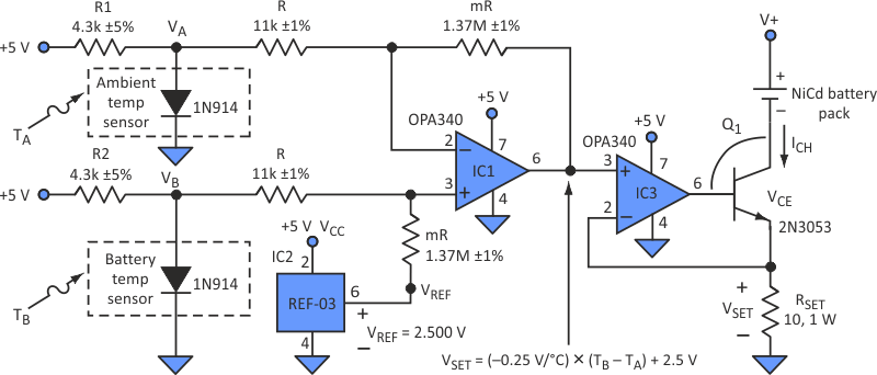
The design begins by writing three linear equations that describe each of the circuit elements depicted graphically. The two temperature-derived diode voltages (Fig. 2) are applied to the inputs of a standard difference amplifier (IC1), which subtracts sensor voltage VA = (–2 mV/°C)TA + 670 mV from VB = (–2 mV/°C)TB + 670 mV to produce a differential voltage (VDIFF):
|
(2) |
In addition to performing the subtraction described by Equation 2, IC1 amplifies VDIFF by a differential gain (ADIFF), determined to be 125, and adds an offset voltage of +2.5 V to the output. The differential amplifier’s performance equation is:
 |
(3) |
The components are selected by simply comparing gain and offset terms to design the needed signal-conditioning circuit described by:
 |
(4) |
Notice that comparing terms also shows how to correctly wire the inputs – i.e., VB must be wired to the V(+) input and VA must be wired to the V(–) input. IC1’s differential gain is:
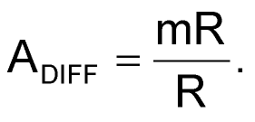 |
(5) |
VREF is set by IC2, a low-output-impedance reference chip (a REF-03) that creates precisely 2.50 V.
The design of the voltage-to-high-current converter starts by noting that ICH is directly proportional to the temperature-dependent voltage, VSET, and circuit performance is:
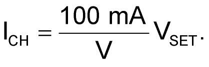 |
(6) |
Finally, note that negative feedback around IC3 forces VSET to be applied directly across the current-setting resistor, RSET, making: