Some transducers for portable or automotive applications need accurately regulated, high-voltage bias and draw little current. To produce such high voltages from a low battery voltage, designers typically use switch-mode dc/dc converters – generally, flyback converters. These converters exhibit high efficiency at medium or high output power. However, for the low output power for biasing some transducers, the fixed amount of power the power-switch driver and the regulator circuitry require can have a detrimental effect on efficiency. Furthermore, the associated transformer is rarely available off the shelf, so it requires a custom-design effort. This effort can account for 70% of the entire design time.
 |
||
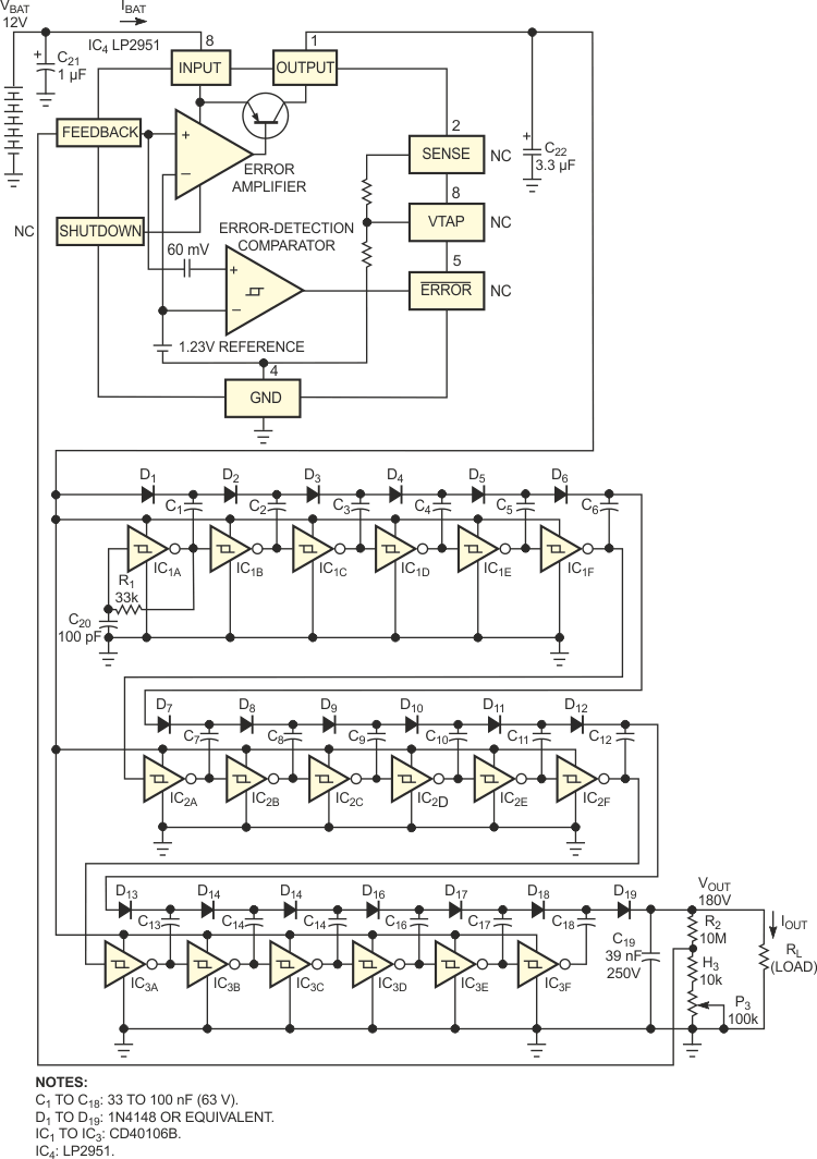
| Figure 1. | This four-IC circuit uses no transformers and converts 12 V to 180 V, using off-the-shelf components. |
|
The circuit in Figure 1 overcomes the transformer-related problem, thanks to a transformerless, switched-capacitor topology that requires only off-the-shelf components. You can describe the operating principles of the circuit by first considering the behavior of a single switched-capacitor cell and then extending the concept to an N-cell voltage multiplier. Figure 2 represents the equivalent circuit of the first switched-capacitor cell.
 |
||
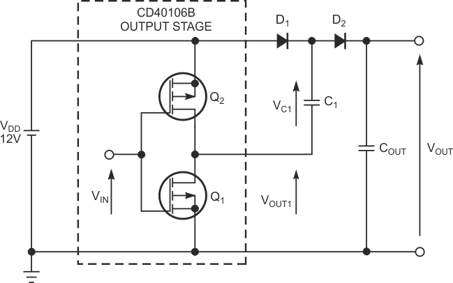
| Figure 2. | This circuit illustrates the operating principle of the basic voltage-doubler cell. | |
The two complementary MOSFETs, Q1 and Q2, mounted in a push-pull configuration, represent the output stage of one CD40106 Schmitt-trigger inverter. The input signal, VIN, drives the push-pull stage, producing a 0 to 12 V square wave at 150 kHz. If you assume that VIN is 12 V during the first half-period, then Q1 is on, and Q2 is off. Consequently, D1 is forward-biased, and C1 charges positively to VC1 = VDD – VD, where VD is D1's forward-voltage drop (0.7 V). Meanwhile, D2 is forward-biased, and COUT charges to VOUT = VDD – 2VD. During the second half-period, the states reverse: VIN is 0 V, Q1 is off, and Q2 is on, thus connecting the negative terminal of C1 to the supply voltage. This action forces the positive terminal of C1 to elevate itself to a voltage higher than the supply voltage, VDD. D1 now becomes reverse-biased and allows C2 to charge up again through D2. If you assume that COUT's value is considerably lower than the value of C1, then you can calculate that VOUT attains the value
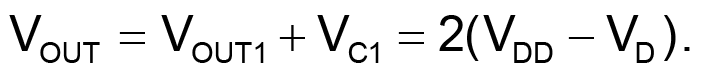
Thus, assuming VDD >> VD, you can see that the circuit in Figure 2 acts as a voltage-doubler cell.
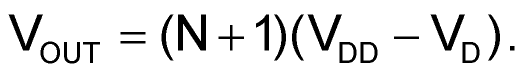
If you cascade N voltage-doubler cells in the chainlike structure of Figure 1, an extension of the voltage-doubler principle yields
 |
(1) |
From this equation, you can determine the number, N, of inverters you need to produce a given high output voltage:
 |
(2) |
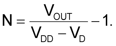
To produce 180 V output voltage from a 12 V lead-acid battery, which can fluctuate from 11 to 13.5 V, an application of the equation (2) with worst-case VDD of 11 V yields
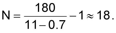
So, your design requires three CD40106 hex Schmitt-trigger inverters, as Figure 1 shows. An inspection of the Equation 1 reveals that the 11 to 13.5 V fluctuation of the lead-acid battery produces a proportional 195 to 243 V output-voltage fluctuation. This variation is unacceptable for biasing applications requiring accuracy. The obvious solution to this problem is to regulate the output voltage, VOUT. You could use either of two regulation techniques: Connect a high-voltage regulator directly to the output terminal, VOUT, or control the low-supply voltage, VDD, of the CMOS inverters to indirectly regulate the output voltage, VOUT. Because of the high cost and low efficiency of linear high-voltage regulators, the circuit in Figure 1 uses the second regulation technique.
| Table 1. | Input regulation at IOUT = 20 µA | ||||||||||
|
|||||||||||
The key element of the feedback loop is the low-cost, low-dropout regulator, IC4, the LP2951. The output of this regulator produces the variable-supply voltage, VDD, to the 16 Schmitt-trigger inverters (IC1 to IC3). With this arrangement, IC4 has to deal with input voltages ranging from only 11 to 13.5 V. The output voltage, VOUT, feeds back to IC4's error amplifier via the resistive divider, R2, R3, and P3. IC1A, the first multiplier cell, produces the square waveform that the 18-cell, switched-capacitor voltage multiplier needs. Using the feedback network (R1, C1), this Schmitt-trigger inverter constitutes a free-running oscillator that produces a 150-kHz square waveform at its output. Table 1 and Table 2 show the measured electrical characteristics of the regulated 12-to-180 V dc/dc converter. The input-regulation characteristic in Table 1 proves that the output voltage does not fluctuate significantly for battery voltages ranging from 11 to 14 V. From the output-regulation characteristic in Table 2, you can see that the overall power efficiency attains 61%, the maximum output current reaches 1 mA, and the peak-to-peak output ripple voltage does not exceed 0.2 V.
| Table 2. | Output regulation and efficiency at VBAT = 12 V | ||||||||||||||||||||||||||||||
|
|||||||||||||||||||||||||||||||