Introduction
In many applications, it is not possible to measure distance to the target by establishing a physical contact. Typical examples include measuring presence of objects on a conveyor belt in logistic centers, or ensuring safety distances around moving robot arms. Other possible options for contactless distance measurement are eddy currents, ultrasounds and light.
Light distance and ranging (LIDAR) systems use the time taken by the light to travel back and forth to an object to measure the distance to this object. A LIDAR system can be built with either a high-speed ADC or a time-to-digital converter (TDC). TDCs can be a timer in a microcontroller/microprocessor (MCU/MPU), dedicated logic on a field-programmable gate array (FPGA), or more simply, a dedicated TDC integrated circuit (IC). This article is an introduction to designing systems based on TDCs and covers optical and analog front-end considerations, as well as basic signal processing for TDCs.
Optical design
To help define an electronic system, here is a list of optical requirements that can impact an electronic system:
- The transmit lens and receive lens field-of-views must overlap. This requirement defines the minimum sensing distance.
- Optical components may be needed to maximize the energy received by the photodiode. This is achieved by focusing the energy on the photodiode’s active area.
- An optical component may be needed to correct the astigmatism of the laser light-emitting diode (LED). Uncorrected, the laser beam will diverge, which reduces the maximum sensing distance. When corrected, the light beam is said to be collimated.
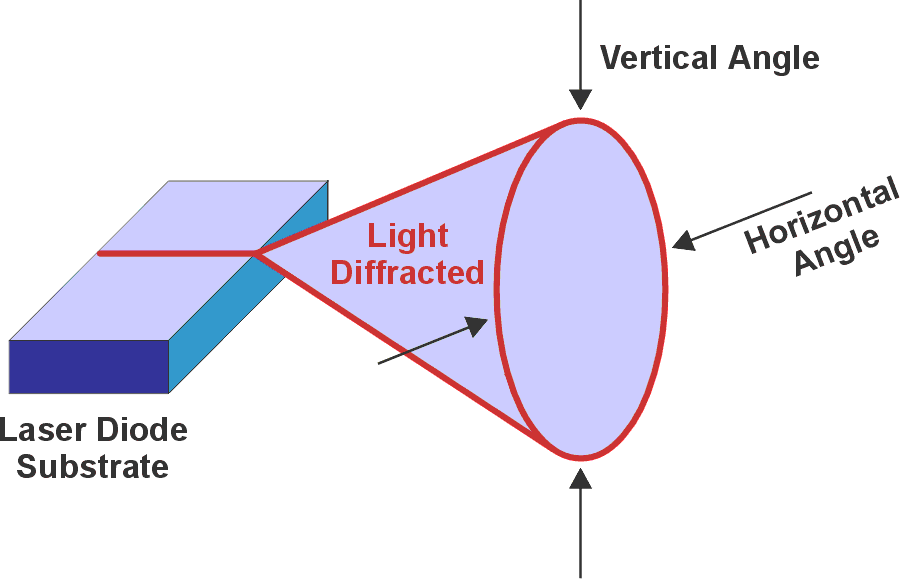
Laser-beam divergence occurs in semiconductor-based laser LEDs because their mechanical structure forces the light to diffract as it leaves the semiconductor substrate. The slit needs to be longer in the horizontal direction than in the vertical direction (Figure 1).
 |
|
| Figure 1. | Horizontal versus vertical diffraction angles of a semiconductor laser LED. |
Most laser LEDs are vertically stacked so that the horizontal slit creates a diffracting beam, which has a wider vertical angle than the horizontal angle.
As a first approximation, consider a diffracted beam angle of 30 to 40 degrees on the perpendicular axis and 10 degrees for the parallel axis. The difference in divergence between the vertical and horizontal axis leads to the astigmatism requirement.
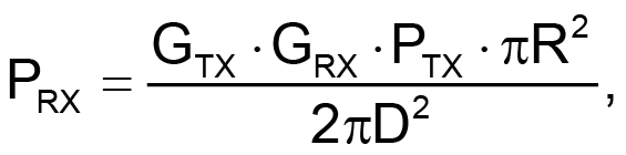
Using the above description, the radar equation can be adapted to a LIDAR system using Equation 1.
 |
(1) |
where:
PRX = the received power by the sensing element of the LIDAR system,
PTX = the transmitted power by the active element of the LIDAR (light output),
GTX = the efficiency of the transmitting element,
GRX = the efficiency of the receiving element,
R = the half-diameter of the optical receiving element (and πR2, the surface),
2π = the solid angle at which light is diffracted by the target, and
D = the distance between the target and the sensing element.
The assumption behind Equation 1 is that all the energy transmitted hits the target. Should this not be the case, in the absence of lenses to correct the divergence of the beam when using LEDs, PRX is then a function of 1/D4 and not 1/D2.
Background light, wavelength and maximum sensing range
To determine the maximum possible amount of sunlight energy that could saturate the receive path, ASTM G173 is a good source [1]. Sunlight on the earth’s surface has a power density of 0.62913 W/m2 at 905 nm. Assuming a receiver lens with a diameter of 1.5 cm, the sensor will receive 1.4 µW when directly facing the sun. This value of 1.4 µW can then be considered as a worst case (which some may consider unrealistic) for signal-chain dimensioning.
While it is important to consider ambient light for gauging the saturation level of the receive path, also consider target reflection and diffractions for gauging receive-path sensitivity. This seems to be the least documented aspect at the system level. Beyond the ISO16331 standard, which mentions a reflection range between 20% and 80%, few other sources are available. According to the Riegl, 905-nm asphalt has the lowest relative reflectance of 10%, while snow has one of the highest relative reflectance of 90% [2].
Eye safety
IEC 60825 [3] is a key consideration for eye safety when designing with lasers. No design should be started without being familiar with this standard.
Having covered generic aspects of a LIDAR system, now consider some of the key electronic subsystems.
Analog front-end (AFE)
To get some initial dimensioning for the frontend, based on Equation 1 and the following assumptions, the power levels received by the photo sensor for various distances are shown by Table 1.
- GTX = 1
Light perfectly collimated and reaches target 100% - GRX = 0.5 A/W
Average value for photo-element sensitivity - PTX = 70 W
Based on existing LIDAR laser diode data sheets - R = 1.5 cm
Radius of the receiver lens
| Table 1. | Power received by the photo sensor versus distance | ||||||||
|
|||||||||
A photodiode generates a small current that is proportional to the received power. A photodiode will typically generate 0.5 A for every watt of received power. In order to generate a voltage that can be used by the rest of the signal chain, a specific amplifier topology is used: a transimpedance amplifier (TIA). This means that a current of 0.4 μA will be generated for a target object at 100 m.
For example, the OPA857 can be used for such an application to provide a built-in gain of 5 k or 20 k (the gains can be selected with a dedicated input of this device). With a gain of 20 k, and at the maximum distance range, an output voltage swing of 8 mV needs to be resolved.
While it is beyond the scope of this article to cover the details of a TIA design, the ability of the TIA to detect a small voltage swing and the comparator offset voltages are specific to LIDAR designs. To design such a circuit, careful considerations are required when choosing the comparator’s input-offset and amplifier’s output-offset voltages.
Considerations for accuracy of the measurements
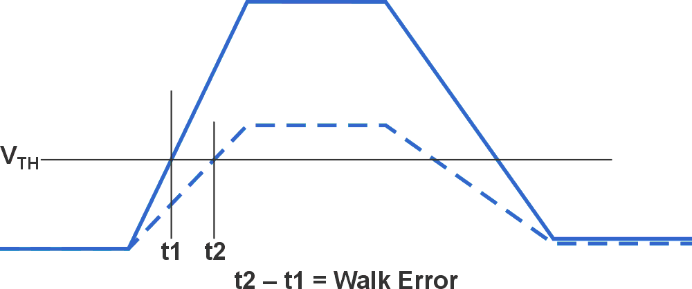
Beyond input noise, electrical noise and jitter, a specific accuracy error for the pulse time-of-flight measurement is called the “walk error” (Figure 2) [4]. The walk error is best understood when considering the impact of variable reflectivity levels on the received signal. Since the rise time of the transmitted signal is finite, the rise time of the received signal will be the same. This means that the received signal needs to pass a given threshold (VTH in Figure 2) at different times (t1 and t2, respectively), depending on its full amplitude.
 |
|
| Figure 2. | Impact of the received amplitude on the estimation of the time-of-flight. |
Signal processing for TDC
Beyond comparing a signal to a threshold before triggering a TDC, not much literature is available on signal processing. Therefore, a few options must be considered to allow more signal processing for TDC-based systems and to further increase their accuracy and robustness.
Signal chain for TDC-based setup
Analog-to-digital converter (ADC) signal processing is taught in all electronic classes and are based on Harry Nyquist’s sampling theory and the later work of Claude Shannon. Shannon’s 1948 paper, “A mathematical theory of communication,” resulted in the creation of the Nyquist-Shannon sampling theorem. [2]
To work with the digital samples coming from a TDC, first look at the problem from another angle. Table 2 gives an overview of the differences and similarities between ADC- and TDC-based sampling.
| Table 2. | Comparison of ADC-based versus TDC-based sampling | |||||||||||||||
|
||||||||||||||||
Before looking into the signal-processing specifics of TDC-generated samples, it is helpful to review a lesser known publication from Bell Labs. In 1976, B.F. Logan published an article, “Information in the zero crossings of bandpass signals,” in which he demonstrates that the zero crossings of h determine h within a multiplicative constant [6]. In other words, if a bandpass signal is captured at the instant at which the signal crosses zero, all information except amplitude is available to reconstruct the signal.
Now, it is reasonable to start building a TDC-based system where the rising edges and falling edges are captured when crossing the zero. This information is all that is needed for digital processing and calculation of the time of flight.
Time-domain correlation
 |
|
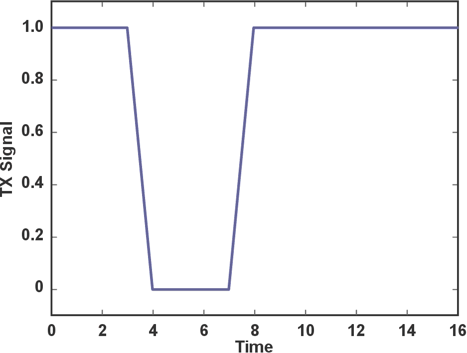
| Figure 3. | Arbitrary transmit pattern 11001111. |
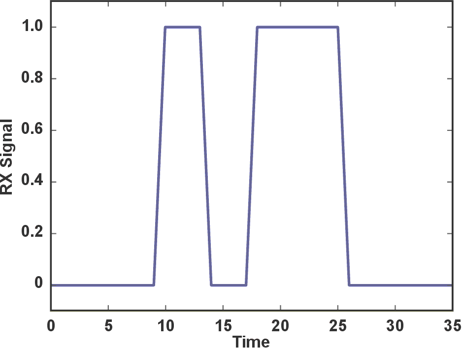
Because there are limited publications about how to use the captured information at zero crossing, a very basic definition can be developed for the signal processing of the information obtained from the rising and falling edges of the TDC. This processing is named time-domain correlation. Time-domain correlation is similar to a classical correlation in that it becomes possible to compute time-of-flight, even in the presence of noise. However, it also differs because the time-domain correlation does not include amplitude information so it must be artificially added. Consider that the signal is 0 before and 1 after a rising edge, and reciprocally 1 before a falling edge and 0 after. Keeping in mind Logan’s theorem, a simple signal reconstruction has been built that is suited to the binary logic of microcontrollers and digital logic. This concept is illustrated in Figure 3 for a typical signal with arbitrary time units. In absence of any noise, Figure 4*) shows the expected output from the comparator.
 |
|
| Figure 4. | The output of the comparator in the absence of noise*). |
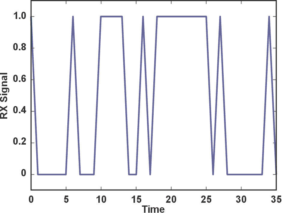
Once the MCU reads the TDC values, the memory will hold [10,+], [14,–], [17,+], etc. The number is the time stamp and the symbol indicates if the edge is rising or falling. A simple subroutine could expand this into an array, which is reflected in Figure 4*). Assuming now that the signal chain is noisy, a possible output of the comparator is shown in Figure 5. The comparator’s threshold should typically be three times above the root-mean-square (RMS) noise floor or more, depending on the compromise between false positive and false negatives. Now the threshold can be lowered significantly, reducing the amount of false negatives.
 |
|
| Figure 5. | Output of the comparator feeding the TDC in the presence of noise. |
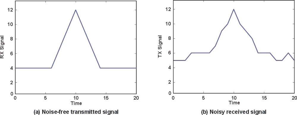
With a classical approach, the MCU subroutine may consider a time-of-flight of five of the arbitrary time units. Figure 6 shows a simple cross correlation between the noise-free transmitted signal and the noisy received signal. Note that the correct time of flight of 10 units is clearly the maximum of the correlation, which is the intended result.
By comparing Figure 6b to Figure 5, a much more robust estimation of the time-of-flight is apparent in Figure 6b. This is because the first rising edge in Figure 5 (or the second or third depending on implementation) is considered the time-of-flight, which can be easily corrupted by noise.
 |
|
| Figure 6. | Correlation between transmitted and received signals. |
A system for time-domain correlation can easily be designed by using two single-channel TDCs (TDC7200) or a single-channel TDC (TDC7201) with each channel being configured for either rising or falling edge.
Conclusion
Developing distance-measurement systems that are based on the time-of-flight with light can be challenging, but also rewarding. To help designers with the decision-making process, this article covered the fundamental aspects of optical designs that are needed to specify the analog frontend. Also addressed were the high-level aspects of the analog front-end and some new ways of leveraging the TDC to build LIDAR systems that use time-domain correlation to achieve improved noise immunity.
References
- “Reference Solar Spectral Irradiance: ASTM G-173,” Renewable Resource Data Center (RReDC)
- Martin Pfennigbauer and Andreas Ullrich, “Multi-Wavelength Airborne Laser Scanning,” ILMF 2001, February 7-9, 2011
- “Safety of laser products - Part 1: Equipment classification and requirements,” International Electrotechnical Commission, IEC 60825-1:2014
- Sami Kurtti, “Integrated receiver channel and timing discrimination circuits for a pulsed time-of-flight laser range finder,” University of Oulu, January 18, 2013
- C. E. Shannon, “A Mathematical Theory of Communication,” The Bell System Technical Journal, Vol 27, pp 379–423, 623–656, July, October, 1948
- B. F. Logan, Jr., “Information in the Zero Crossings of Bandpass Signals,” The Bell System Technical Journal, Vol 56, pp 487-510, April 1977
- M. Amann, T. Bosch, R. Myllyla, M. Lescure and M. Rioux, “Laser ranging: a critical review of usual techniques for distance measurement,” SPIE Digital Library, Opt. Eng. 40(1), 10-19, Jan 01, 2001
*) Figure 4 is the same as Figure 3, except delayed by five time units.