Many single-supply applications need precision amplifiers that can operate from 5 V or lower. Although many precision, single-supply op amps are currently available for configuring as 2- and 3-amplifier instrumentation amplifiers (IAs), these designs require great attention to detail to achieve accuracy and precision. Furthermore, although single-supply IA ICs are available, these products trade off dc and ac performance for low-supply-voltage and -current operation. Dual-supply IAs still offer the best performance.
Achieving high-precision performance in a single-supply application is practical, because the majority of sensor applications provide an output signal centered about the midpoint of a circuit's supply or reference voltage. Examples include strain gauges, load cells, and pressure transducers. In these applications, the signal-conditioning circuitry is not required to operate near the sensor's or circuit's positive supply voltage or ground. Even though the signal-conditioning circuitry need not operate at the extremes of the input-voltage range, the output-voltage swing of the circuitry should be as large as possible to achieve maximum dynamic range. The circuit in Figure 1 achieves high-precision performance while operating from a 5 V supply.
 |
||
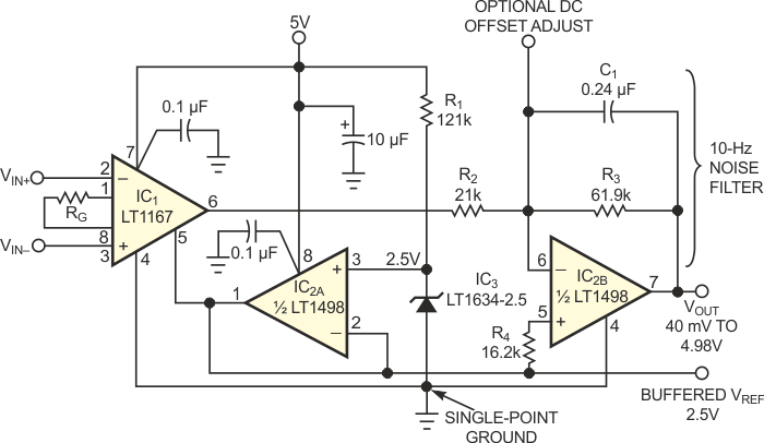
| Figure 1. | A 2.5 V reference IC provides a stable supply midpoint to configure a single-supply instrumentation amplifier. | |
The trick here is to reference the dual-supply IA's inputs to a stable supply midpoint, then follow the IA with a single-supply precision op amp with a rail-to-rail output swing. This “composite” IA uses IC1, an LT1167 high-performance IA, for the input stage, and IC2, an LT1498 high-speed, rail-to-rail input/output dual op amp for the output stage. IC3, an LT1634 micropower 2.5 V precision shunt reference, provides a stable 5 V-supply midpoint. The output of IC3 connects to the input of IC2A, configured as a voltage follower. The output of IC2A provides a low-impedance source for IC1’s reference pin 5, which exhibits 20-kΩ input resistance and input current to 50 µA maximum. A low-impedance source is necessary to maintain IC1’s high common-mode rejection. In addition, IC2A’s output stage can provide load currents to 20 mA for additional external circuitry without affecting IC3’s accuracy.
IC2B is a gain-of-3 inverter whose output can swing ±2.5 V (rail-to-rail) with only ±0.82 V drive from IC1. The primary reason for choosing an inverting-amplifier configuration for the output stage is to make system dc-offset adjustments available. You can connect trim networks to the inverting terminal of IC2B without affecting the static or dynamic behavior of the circuit. However, you should design the trim range so as to not adversely affect the output dynamic range of the circuit.
IC1 maintains its high-linearity performance with a 5 V supply because its front end is configured to operate from dual supplies, and the circuit in Figure 1 relaxes its output drive level. Because IC3 level-shifts the entire circuit above ground, you measure the circuit's final output voltage with respect to 2.5 V, not 0 V. An expression for the gain of this composite IA combines the gain equations of IC1 and the gain-of-3 inverter:
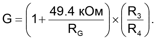
As shown in Figure 1, choosing RG =1.5 kΩ yields a gain-of-100 composite configuration. You can obtain other gain values with different values of RG, as shown in Table 1. Even though it's not necessary that the inputs to the circuit operate at the positive rail or ground, wide input common-mode operation is always beneficial.
| Table 1. | Summary of static and dynamic characteristics | ||||||||||||||||||||||||||||||
|
|||||||||||||||||||||||||||||||
| * Referred to input | |||||||||||||||||||||||||||||||
In this configuration, IC1’s input stage can accept signals as high as 3.7 V (common mode plus differential mode) with no loss of precision. In fact, at low circuit gains, the circuit's common-mode input-voltage range spans 2.25 to 3.45 V. This wide common-mode range allows room for the full-scale differential input voltage to drive the output ±2.5 V about the reference point (VREF). Another application hint regarding this circuit: Though IC1’s input bias currents are lower than 1 nA, the circuit's differential-input terminals must have a dc return path to the power supply.
Table 1 summarizes the static and dynamic performance of the composite IA. Nonlinearity for all gain values is lower than 0.006%. The transient response of the circuit as a function of gain and load is well-behaved and is attributable to IC2’s wideband rail-to-rail output stage. Note that measurements of small/large-signal transient response and circuit bandwidth reflect the absence of C1. The circuit's 10-MHz gain-bandwidth product and 6 V/µsec slew rate ensure that the small-signal performance is primarily a function of IC1’s characteristics. Capacitor C1 is beneficial in low-frequency applications (signal bandwidth lower than 20 Hz), to eliminate or significantly reduce noise pickup. Noise can also sneak into the circuit via the input terminals of IC1, especially if the sensor is located some distance from the signal-conditioning circuitry. This type of noise can cause a shift in the input offset voltage of IC1, thereby producing errors. This effect is commonly termed RF rectification. You can easily add a differential filter to IC1’s input terminals to reduce this effect.