The need for conditioning low-level ac signals in the presence of both common-mode noise and differential dc voltage prevails in many applications. In such situations, ac-coupling to instrumentation and difference amplifiers is mandatory to extract the ac signal and reject common-mode noise and differential dc voltage. This situation typically occurs in bioelectric-signal acquisition, in which metallic-electrode polarization produces a large random differential dc voltage, ranging from ±0.15 V, which adds to low-level biological signals. Input ac-coupling is one approach to removing the differential dc content. But this technique requires adding a pair of capacitors and resistors to ac-couple the inputs of the difference amplifier. The manufacturing tolerances of these components severely degrade the CMRR (common-mode-rejection ratio) of the amplifier. If cost is not an issue, you could perform an initial trim, but this operation is useless for biological applications plagued by wide variations in electrodes and tissue impedances. The differential topology in Figure 1 addresses these problems (Reference 1).
 |
|
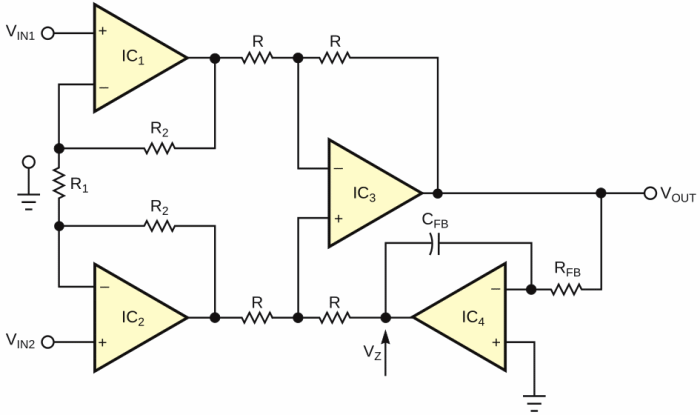
| Figure 1. | This ac-coupled instrumentation amplifier accommodates only ±5-mV maximum input. |
The principle of this ac-coupled instrumentation amplifier is to maintain the mean output voltage at 0 V. To do so, you insert an autozero feedback loop, comprising IC4, RFB, and CFB, in a classic three-op-amp instrumentation amplifier. This feedback loop produces a frequency-dependent transfer function:
Consequently, the ac-coupled instrumentation amplifier behaves as a highpass filter with a –3-dB cutoff frequency from the equation
At first glance, you might think that the output-autozeroing behavior of the ac-coupled instrumentation amplifier is perfect. Unfortunately, the output autozeroing capability of this circuit is strongly limited. You can determine this limitation by expressing the output voltage as a function of the input signals and the integrator's output voltage, VZ:
where VOUT is the output voltage. In this expression,
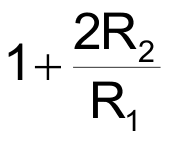
is the differential gain in the passband. At dc, the output voltage is 0 V as long as the integrator's output does not reach its saturation voltage, VZ(MAX). Therefore, setting the output voltage at 0 V in the above expression yields the maximum differential-input dc voltage that this circuit can handle:
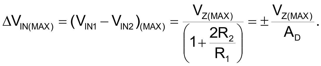
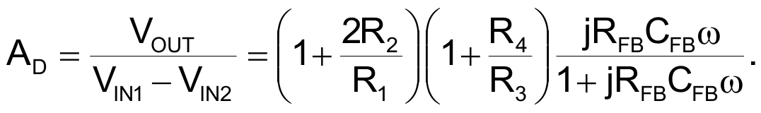
Consider, for instance, the typical performance and constraints of a portable biotelemetry system: differential gain of 1000, ±5 V split power supplies, and op amps with rail-to-rail output-voltage swing. In this system, the application of the formula for ΔVIN yields a maximum differential-input dc voltage of only ±5 mV. This limited performance is unacceptable for biological applications, in which you encounter differential-input dc voltages of ±0.15 V. The ac-coupled instrumentation amplifier in Figure 2 overcomes this limitation, thanks to the addition of "active feedback," which includes voltage divider R3-R4 and the associated buffer amplifier, IC5. With this arrangement, the following equations give the new transfer function and highpass cutoff frequency, respectively.
The expression for the output voltage as a function of the input signal and the integrator's output voltage, VZ, becomes:

In this expression,
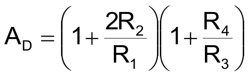
is the new differential gain in the passband.
At dc, the output voltage remains 0 V as long as the integrator's output does not reach its saturation voltage, VZ(MAX). Therefore, setting the output voltage at 0 V in the new expression for output voltage yields the new maximum differential-input dc voltage and differential gain. They are, respectively:
and
In the above equations, the additional term, 1+R4/R3, is the gain of the active-feedback stage.
The new expressions for ΔVIN(MAX) and AD(MAX) clearly show the advantages of Figure 2's ac-coupled instrumentation amplifier with active feedback: For an identical differential gain, you can extend the polarization-voltage range, ΔVIN(MAX), by a factor equal to the gain of the active-feedback stage. Conversely, for a given polarization-voltage range, ΔVIN(MAX), you can increase the differential gain by the gain of the active-feedback stage.
 |
|
| Figure 2. | This instrumentation amplifier can accommodate a differential-input range of ±0.34 V. |
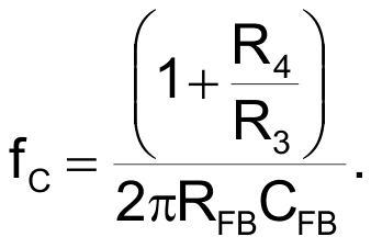
The only drawback of this topology is apparent in the expression for fC, the highpass cutoff frequency. You multiply this frequency by the gain of the active-feedback stage. Therefore, to maintain a given cutoff frequency, you must multiply the time constant by a factor equal to the active-feedback stage gain. This factor can be an issue in processing signals whose spectrum includes low-frequency components. In such applications, RFB and CFB can reach prohibitive values. Consequently, you must make a trade-off between the time constant and the active-feedback stage gain. The component values in Figure 2 are a typical example of such a trade-off: The values are for an EEG (electroencephalogram) amplifier with ±5 V split power supplies. The amplifier has a differential gain of 1000 and a highpass cutoff frequency of 2.3 Hz, and it can handle a differential-input dc-voltage range of ±0.34 V.
To obtain this performance, you set the active-feedback stage gain and the differential-amplifier gain, respectively, to 67.6 and 15. With these gain values, the noise performance of the ac-coupled instrumentation amplifier of Figure 2 is similar to that of a classic instrumentation amplifier. This situation occurs because the autozeroing and active-feedback stages, IC4 and IC5, are after the input differential stage, IC1 and IC2. Consequently, the gain of the differential stage roughly divides their respective noise contributions, which are therefore negligible. You can use several low-noise op-amps for IC1 and IC2. For portable biotelemetry applications, the LT1464 is a good compromise for input-noise density, noise-corner frequency, input-bias current and current drain. (Respectively: VNOISE=26 nV/√Hz, fC=9 Hz, IBIAS=0.4 pA, and ICC=230 μA.)
A theoretical analysis using the LT1464's noise parameters shows that under worst-case conditions, the input-noise voltage should not exceed 11 µV rms. Tests on prototypes confirm this prediction; the tests effectively measure input-noise voltages of 3 to 6 µV rms. To sum up, an ac-coupled instrumentation amplifier with active feedback is well-suited for applications requiring high differential gain, a capability for handling large differential-input dc voltages, and low-noise performance.