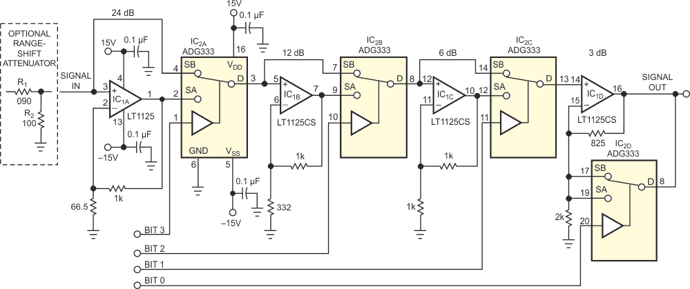
A number of single-chip VGAs variable-gain amplifiers are available today. Unfortunately, they all have drawbacks, such as high noise, 55 V limit, low input impedance, or nonlinear gain/frequency characteristics. The circuit in Figure 1 is a 16-step, ultralow-noise VGA that solves many of these problems. IC1 is a low-noise quad op amp, and IC2 is a quad SPDT CMOS switch. The stages switch in successive multiplication (gain) factors using a TTL binary code. The values shown provide 0- to 45-dB gain in 3-dB steps. For best low-noise performance, the higher gain stages precede the lower gain stages. The circuit exhibits approximately 3 nV/√Hz referred to the input, for most gain settings. The highest noise is 4.5 nV/√Hz at a gain of 9 dB. Distributing the total gain across multiple stages increases the overall bandwidth. The output stage has a different configuration to yield a low-output-impedance output driver at all gain settings.
 |
|
| Figure 1. | This VGA offers ultralow noise, a wide dynamic range, and high bandwidth. |
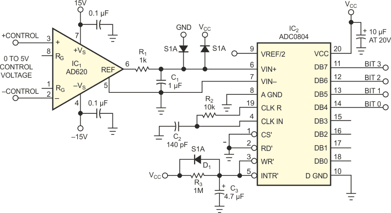
If you need to remotely control the gain, you must concern yourself with ground loops that can compromise the low-noise characteristics of the circuit. One solution is to place optoisolators in the four digital-control lines, so that no ground connection exists between the two ends of the cable except through the power supply. The method you use is an analog differential-control voltage using an ADC to generate the 4 bits. Figure 2 shows a circuit that performs this function well. IC1 is a differential receiver, and IC2 is an 8-bit ADC. In some applications, you could get away with using only the ADC, because it already has a differential input. However, you must take care not to exceed the narrow common-mode range of the ADC's input. A more robust solution is to place a differential receiver in front of the ADC, as shown. R1 and C1 form a lowpass filter for the control voltage to the ADC. The 4 high-order bits from the ADC control the CMOS switches. As shown, the ADC operates in a self-clocking mode and needs no other controls.
 |
|
| Figure 2. | An ADC controls the gain-setting codes for the circuit in Figure 1. |
R2 and C2 control the sampling frequency, approximately 640 kHz for the values shown. D1, R3, and C3 provide power-up initialization for the ADC's clocking function. The control-voltage steps are 310 mV apart, providing ample noise immunity. Table 1 shows the performance of the overall circuit with analog control. You can use R1 and R2 in Figure 1 to shift down the overall gain range with little sacrifice of noise characteristics. You can obviously alter the individual gain stages to yield other ranges and step sizes, such as 0 to 30 dB in 2-dB steps. At the expense of circuit simplicity, you could replace the quad op amp with four ultra-low-noise op amps, such as the LT1128 or AD797. This replacement lowers the noise to approximately 1.4 nV/√Hz.
| Table 1. | Performance versus gain | |||||||||||||||||||||||||||||||||||||||||||||||||||||||||||||||||||||||||||||||||||||
|
||||||||||||||||||||||||||||||||||||||||||||||||||||||||||||||||||||||||||||||||||||||
You could also increase the number of stages, thereby providing a wider dynamic range, finer gain steps, or both. The benefits of this circuit over commercially available single-chip VGAs include ultra-low noise, high bandwidth, ±13 V range, high input impedance, ground-loop immunity, and user-defined dynamic range and step size.