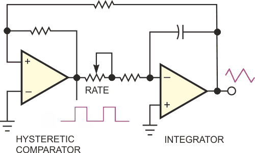
The circuit in Figure 1 is a variation on the familiar integrator/comparator triangle-wave oscillator, which you typically implement with two op amps. An integrator and a comparator connect in a positive-feedback loop; the comparator drives the integrator and vice versa. A fixed amount of hysteresis exists in the comparator, producing a triangle wave at the integrator’s output. The wave oscillates between the fixed threshold voltages. You can vary the oscillation rate using a potentiometer to set the integrator’s gain and thus obtain a constant-amplitude, variable-frequency, triangle-wave output. In the circuit of Figure 2, the integrator’s gain is fixed, whereas the comparator’s hysteresis is variable. An OTA (operational transconductance amplifier), IC2, sets the hysteresis, producing an oscillator in which the period is a linear function of an externally applied voltage. The oscillation rate is inversely proportional to the control voltage; in other words, the oscillator has a 1/x response. Such an oscillator is useful in A/D-converter applications and for clocking time-delay systems, such as audio-delay lines.
 |
|
| Figure 1. | This circuit is a classic triangle-wave generator, using an integrator and a comparator with hysteresis. |
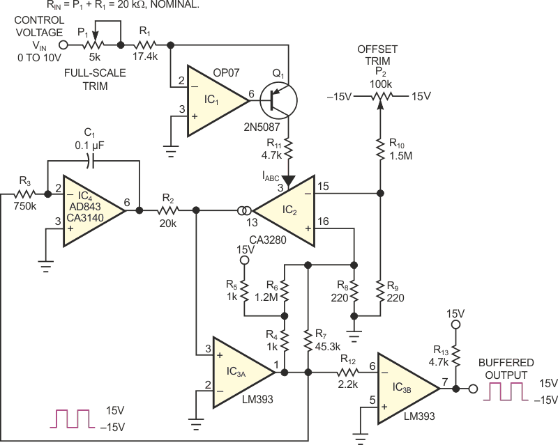
In Figure 2, R3 and the ±15 V output of comparator IC3A fix the integrator current at ±20 µA. The integrator produces a triangle of fixed ±200 V/sec slope, and the peak amplitude is a function of the hysteresis. OTA IC2 provides voltage control of the hysteresis. With increasing VIN, the hysteresis and triangle-wave peak-to-peak amplitude increase, consequently increasing the oscillator period, T. The triangle wave’s amplitude changes from approximately 1 mV p-p to a maximum of 20 V p-p as VIN varies from 0 to 10 V. With the same VIN span, the period increases from 20 µsec to 200 msec. IC1 and Q1 form a linear voltage-controlled current source that supplies bias current, IABC, to the OTA. The current
You can see that IABC increases from 0 to 0.5 mA as VIN varies from 0 to 10 V. The OTA is a switched-current generator, producing a bidirectional output current approximately equal in amplitude to IABC, when it receives drive from the comparator’s open-collector output.
 |
|
| Figure 2. | This VCO uses an OTA and a hysteretic comparator to deliver a reciprocal (1/x) response to the control voltage. |
The OTA sources current when the comparator’s output is 15 V and sinks an identical current when the output is –15 V. Pullup resistors R4 and R5, along with resistors R6 through R9, provide a symmetrical ±70 mV drive to the OTA’s noninverting input. The high-compliance output of the OTA provides hysteresis by translating the voltage at the comparator’s noninverting input up and down by the amount
The resulting threshold voltages are symmetrical around the comparator’s input offset voltage. This symmetry reduces the effect of offset voltage on the oscillator’s period. This design uses an LM393 comparator for its relatively low maximum bias current of 25 nA. The comparator’s output changes state when the integrator’s output begins to exceed the threshold voltage set by hysteresis, reversing the direction of the OTA’s output current and the threshold polarity. This action makes the integrator’s slope reverse and initiates the next half-cycle.
You can calculate the oscillator’s period as follows:
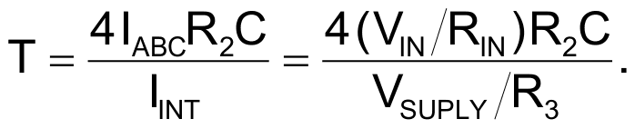
For the given component values,
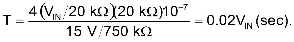
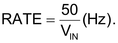
Potentiometer P1 sets the full-scale period for VIN = 10 V, and P2 nulls the OTA’s input offset voltage to optimize the performance at small values of VIN. With the component values shown, the circuit covers a three-decade range from 200 µsec to 200 msec with lower than 1% linearity error. The error increases to 2% for T = 100 µsec. With a 10-nF integrator capacitor, the circuit oscillates at frequencies as high as approximately 150 kHz (T = 6.7 µsec). The CA3280 OTA provides the best performance in this circuit, thanks to its excellent offset specifications. Using the CA3080 and LM13600 in the circuit reduces performance. The integrator op amp should have low input-bias current and high-speed response to minimize ringing on triangle peaks. The AD843 and CA3140 both work well. You could add temperature compensation by including a thermistor in the OTA’s input-attenuator circuit. Finally, note that you should use polystyrene or polypropylene capacitors in the integrator.