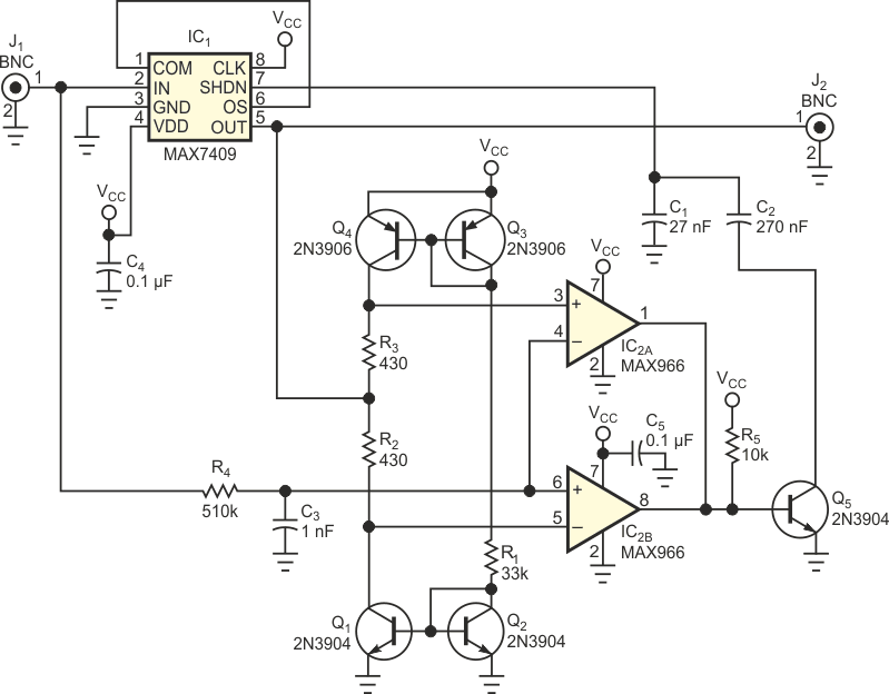
A common problem that arises when you design lowpass filters for signal conditioning is the filters' effect on the system's time-domain response. Because pushing the cutoff frequency lower slows the step response, the system may fail to recognize significant changes within a reasonable amount of time. The circuit in Figure 1 accommodates lower cutoff frequencies without sacrificing the step-response time. A window comparator monitors the delta (difference) between the filter's input and output. When the delta exceeds ±50 mV, the filter increases its slew rate by increasing the cutoff frequency by an order of magnitude. The switched-capacitor filter, IC1, normally operates as a self-clocked device. Capacitors C1 and C2 set the cutoff frequency at 0.1 Hz, and other circuitry forms a dynamic window comparator. Transistor pairs Q1-Q2 and Q3-Q4 form a complementary current mirror whose output flows through R2 and R3, creating a delta of ±50 mV. Connecting the output voltage to the center tap of the two resistors centers the delta on the output voltage. You therefore set the window comparator's upper threshold at VOUT + 50 mV and the lower threshold at VOUT – 50 mV.
 |
|
| Figure 1. | This lowpass filter maintains a fast step response by dynamically adjusting its cutoff frequency. |
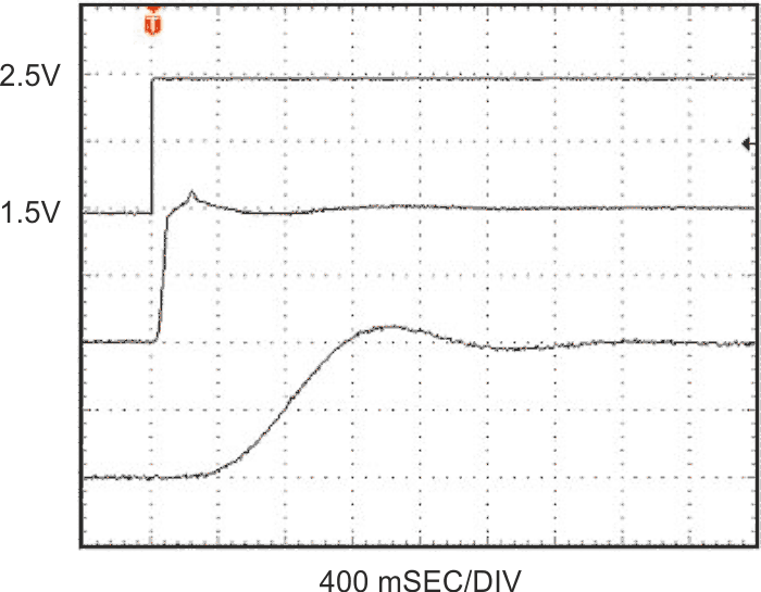
R4 and C3 provide lowpass-filtering to the original input signal, producing a 312-Hz cutoff frequency that reduces sensitivity to momentary glitches. The filtered input drives the window comparator's input. If that input is outside the ±50-mV window, comparator IC2A or IC2B asserts its output low. The low output drives Q5 into cutoff, causing its collector to assume a high impedance. Because Q5’s collector no longer grounds capacitor C2, the filter's cutoff frequency increases by a factor of 10. When the system's output changes to within 50 mV of the input, the cutoff frequency throttles back to its quiescent state. Figure 2's oscilloscope photo shows the effect. The top trace is a step from 1.5 to 2.5 V, the middle trace is the output with optimization circuitry enabled, and the bottom trace shows the filter's unmodified response. The optimized response includes a slight perturbation during the cutoff-frequency transition, but is five times faster than that of the unmodified circuit. The circuit in Figure 1 is configured for low cutoff frequencies, but you can rescale it for higher frequencies by changing C1 and C2. You can also modify R2 and R3 for different window values, for which the delta equals the resistance multiplied by 115 µA. The comparator must be an open-drain type.
 |
|
| Figure 2. | These traces show the time-domain response for the circuit in Figure 1 with optimization circuitry (middle trace) and without it (bottom trace). |