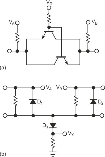
Interfacing two systems that operate at two arbitrary voltages is a challenging problem; there is no guarantee that one side operates at a voltage higher than the other side. Usually, the interface is an open-collector or open-drain type with just two transistors connecting back to back (Figure 1a). VX is the lower of the two operating voltages. If you know which side has the lower operating voltage, the interface design is straightforward. If either side can have the lower operating voltage, you have to extract the lower one. Without the use of an op amp, you can use a diode-based circuit (Figure 1b). The 1N4148 is good for most applications. If a higher current capability is necessary, you can use the 1N4001. If the lower operating voltage is around 1 V, D3 should be a Schottky diode, such as the 1N5817 or MMBD701, and D1 and D2, can be normal PN-junction diodes.
 |
|
| Figure 1. | An open-collector or open-drain circuit (a) typically interfaces between two systems that operate at two arbitrary voltages. A diode-based circuit (b) can extract the lower operating voltage. |
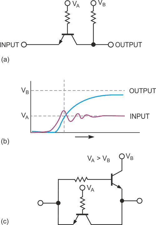
If level translation is necessary in one direction, you can use half of the circuit for open-drain translation, which is equivalent to simple TTL. This simple circuit is fast (Figure 2a). When driving one standard load on a real pc board, which has approximately 10 to 20 pF of total load capacitance, the rise and fall times are fast when you view it with a scope. Circuit performance is better than that of the traditional bipolar inverter, which needs a compensation capacitor to assist turn-off. (Replacing the bipolar transistor with an enhancement MOSFET can eliminate the capacitor but results in long rise and fall times and a longer delay.) The TTL-like circuit uses only pullup resistors, which may further save pc-board space because you can use multiple pullup resistors in one resistor pack.
For a logic high-to-low transition, the delay is just the turn-on time of the transistor. For a low-to-high transition, RC effects don’t appear until the output rises to about 0.5 V below the lower supply voltage, VX, when translating up (Figure 2b). Before that, the output tracks the input with only a VCE(SAT) drop, which is analogous to a cascode amplifier. The effect of turning off a saturated transistor does not manifest itself except when translating from below 1 V to 5 V.
 |
|
| Figure 2. | Level translation in one direction requires half of the open-drain translation circuit (a). For a low-to-high transition, RC effects do not appear until the output rises to about 0.5 V below the lower supply voltage (b). The circuit also works for translating from high to low voltages (VB < VA), and you can replace the resistor with an active pullup (c). |
The TTL-like circuit in Figure 2a also works well for translating from high to low voltages (VB < VA). For a high-to-low transition, the delay is just the turn-on time of the transistor. You can replace the pullup resistor by an active transistor to increase driving strength (Figure 2c).You must pay attention to VEBO(BR), which must not exceed the rated value because a violation results in premature failure of the transistor. For most small signal transistors, VEBO(BR) is typically 4 to 5 V. Therefore, you should take care when down-shifting from 12 to 5 V, such as between CMOS analog circuits and 5 V logic.
 |
|
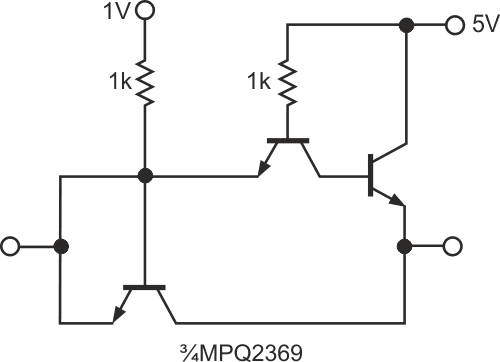
| Figure 3. | The ultimate 1-to-5V up-shifting driver in the laboratory produces a symmetrical delay of 6 nsec using three-fourths of an MPQ2369 when driving a single 74AC541 buffer. |
The switching transistor can be MPS2369A to MPS3646 for high-speed switching. You can use the 2N3904 or BC547 for low-power applications. A 2N5458 can replace the pullup resistor at the collector if active pullup is necessary. The best 1-to-5V shifting driver in the laboratory produces a typical symmetric delay of 6 nsec using three-fourths of an MPQ2369 when driving a 74AC541 buffer (Figure 3).