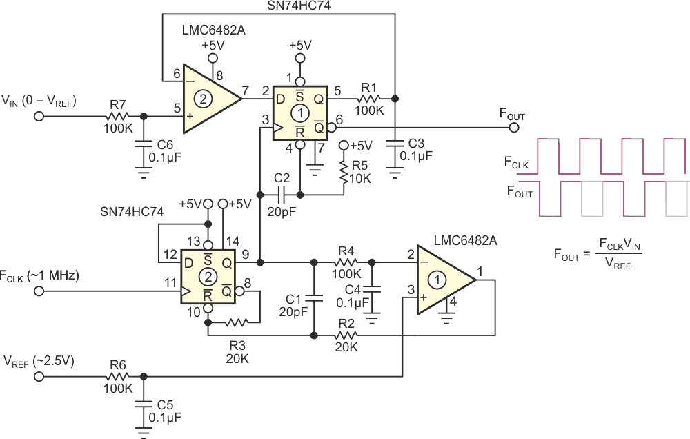
Voltage to frequency converters (VFCs) are a popular method of noise-tolerant analog to digital conversion. Synchronous VFCs (like the Analog Devices AD652) in which an external, usually crystal-derived, clock provides timing for the conversion process, have significant performance advantages (speed, linearity, precision independent of passive components) over the free-running type in which conversion timing must ultimately rely on an RC time constant.
But a characteristic limitation of all VFCs, both synchronous and asynchronous, is that they make relatively slow analog-to-digital converters (ADCs) because the full-scale output frequency, and therefore conversion speed for any given conversion resolution, is limited by the analog switches used in the conversion process in which speed and precision are inherently inversely related. This design idea (Figure 1) pushes maximum accurate operating frequency beyond 1 MHz by utilizing high-speed H-CMOS logic devices as extremely fast analog switches.
 |
|
| Figure 1. | The high speed synchronous VFC. |
Here’s how it works:
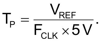
D-type flip-flop #1 (FF#1) in the HC74 forms a feedback loop with op-amp #2 in the 6482 acting as a high-resolution comparator and with the high speed (~ns transition times) of the HC74 switches acting to apply 0/5 V to Q1 according to the 0/1 state of the op-amp output when the FF is clocked. The duty cycle (DC1) of the FF is thus time averaged by R1C3 and servoed by the feedback loop to force
and
But a logic supply is typically a poor choice for a conversion reference voltage, so if this were all there was to the story, expectations for VFC accuracy would likewise be poor. We need a trick to compensate for the inevitable inaccuracy and noise in the +5 V supply.
The needed compensation is provided by FF#2 implementing another feedback loop.
FF#2 is connected to form a monostable (one-shot) triggered by FCLK, applying 5 V pulses to the R4C4 averaging network with pulse duration (TP) determined by R2, R3, C1 network and op-amp #1. The voltage is averaged by
Op-amp #1 compares this average to VREF and forces TP so that
Because both FFs occupy the same chip, accuracy-affecting parameters like propagation delays, transition times, and voltage offsets will be very similar and track well over temperature and supply voltage variations, making compensation very effective.
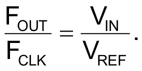
These TP duration pulses become the clock reference for FF#1, thus…
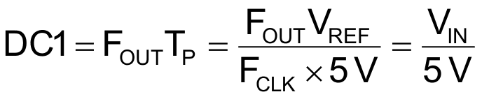
…yielding (finally) the hoped-for classical synchronous VFC conversion equation…
The resulting VFC has some useful characteristics besides high speed (for a VFC). This includes a good linearity, a tolerance of VREF in the range of 1 to 4 V, F from 500 kHz to 3 MHz, operation from a single “5V+”, a 3 to 6 V supply, a low power consumption (~10 mW), very high input impedances (e.g., less than 1 pA input current on VIN and VREF), and no critical or high-precision passive components.
Finally, all parts needed to build it are generic, readily available, and cheap! Total parts cost is ~$10, while by contrast the similar speed AD652, by itself, costs ~$40.