This design idea presents a practical circuit that implements synchronous detection to amplify small DC voltages with high linearity and excellent noise immunity. Such circuits are required in measurements involving current shunts, load cells, thermocouples, etc. Synchronous detection is explained in many books, papers and instrument manuals. If you are not familiar with the topic, reference 1 is a good starting point.
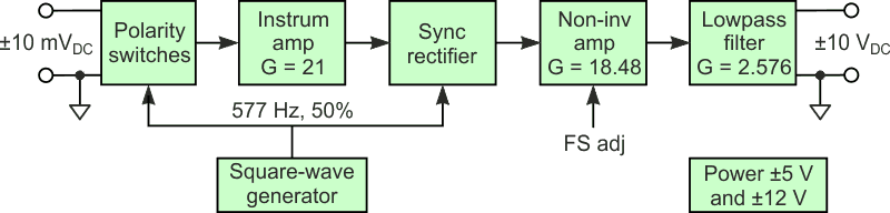
Figure 1 shows the block diagram of the amplifier. It provides a fixed gain of 1000 split between an instrumentation amplifier, an adjustable non-inverting amplifier and a lowpass filter. Polarity switches and the instrumentation amplifier convert the DC input into a bipolar square-wave signal, so the synchronous detection technique can be applied.
 |
|
| Figure 1. | Block diagram of the amplifier. |
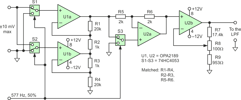
Figure 2 presents the circuits of the first four units of the block diagram. High quality op-amps provide ultra-low offset voltage, very low noise and slew rate of 20 V/µs. All resistors have 1% tolerance, but the R1 to R6 resistors are matched in pairs to 0.05%.
 |
|
| Figure 2. | Circuit schematic of part of the amplifier (filter is presented separately below). |
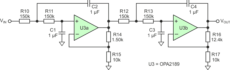
Figure 3 shows the filter schematic. It is a canonical design of a 4-pole Sallen-Key lowpass filter with a DC gain of 2.576 (reference 2), with a cutoff frequency of 1 Hz and row-off rate of –80 dB/dec.
 |
|
| Figure 3. | Schematic of the low-pass filter. |
The square-wave oscillator is based on the 74HC4060 chip. The frequency is set to 577 Hz, a prime number roughly equally spaced between the closest 50-Hz and 60-Hz harmonics.
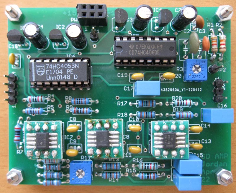
Figure 4 shows the PCB. It is a two-layer board, 78 mm by 62 mm (3.07” × 2.44”) in size. All analog grounds use individual traces connected to a single point at the power supply ground. All measurements are referred to this common point.
 |
|
| Figure 4. | The two-layer PCB of the amplifier. |
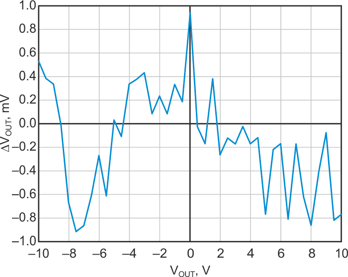
The circuit performance is evaluated with a home-made voltage calibrator (reference 3) and a 6.5-digit multimeter. A 100:1 divider is placed between the two boards to increase input voltage resolution.
The transfer function is approximated with a best fit line; line equation is as follows:
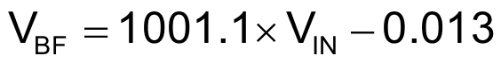
Figure 5 displays deviation between the experimental data of VOUT and the best fit line. The error is between +1 and –1 mV. Referred to the full scale voltage of 10 V, this is an excellent result. The 13 mV offset in the transfer function can easily be canceled by hardware or, if the circuit is connected to a microcontroller, via firmware.
 |
|
| Figure 5. | Circuit performance: deviation between experimental data and the best fit line is within the ±1 mV range. |
To conclude, there are some measures you can apply to improve cost and performance:
Keep the wires connecting the signal source to the board as short as possible.
A cheaper op-amp with less extreme offset voltage specification may be used for U3.
If possible, go with a 2-pole filter. The second op-amp in the package can be used to cancel the offset of the transfer function.
Using SMD parts will reduce the size and the price of the PCB.
References
- Orozco L. Use synchronous detection to make precision, low level measurements. Technical article MS-2698 from Analog Devices.
- Smith S. The scientist and engineer’s guide to digital signal processing. 2nd edition, Chapters 3 and 32, California technical publishing, 1999.
- Dimitrov J. DCV calibrator & reference has under 70 µV error. EDN, DIY, May 26, 2017.