Almost all precision voltage-to-frequency converters (V-F) utilize charge pump based feedback for stability. These schemes rely on a capacitor for stability. A great deal of effort towards this approach has resulted in high performance V-F converters (see Reference 1). Obtaining temperature coefficients below 100 ppm/°C requires careful attention to compensating the capacitor’s drift with temperature. Although this can be done, it complicates the design. Similarly, capacitor dielectric absorption causes errors, limiting linearity to typically 0.01%.
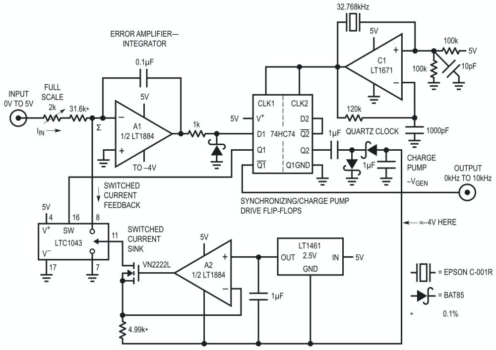
Figure 1’s 5 V powered design, derived from Reference 1’s ±15 V fed circuit, reduces gain TC to 8 ppm/°C and achieves 15 ppm linearity by replacing the capacitor with a quartz-stabilized clock.
 |
|
| Figure 1. | 5 V powered, quartz-stabilized 10 kHz V-F converter has 0.0015% linearity and 8 ppm/°C temperature coefficient. A1 servo controls A2 FET switched current sink via clock synchronized flip-flop to maintain zero volt summing junction (Σ). Loop repetition frequency directly conforms to input voltage. |
In charge pump feedback-based circuits, the feedback is based on Q = CV. In a quartz-stabilized circuit, the feedback is based on Q = IT, where I is a stable current source and T is an interval of time derived from a clock. No capacitor is involved.
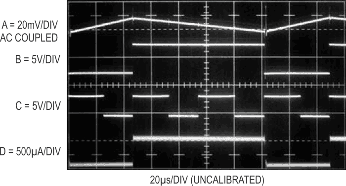
Figure 2 details Figure 1’s waveforms of operation. A positive input voltage causes A1 to integrate in the negative direction (trace A, Figure 2). The flip-flop’s Q1 output (trace B) changes state at the first positive-going clock edge (trace C) after A1’s output has crossed the D input’s switching threshold. C1 provides the quartz-stabilized clock. The flip-flop’s Q1 output controls the gating of a precision current sink composed of A2, the LT1461 voltage reference, a FET and the LTC1043 switch. A negative bias supply, derived from the flip-flop’s Q2 output driving a charge pump, furnishes the sink current. When A1 is integrating negatively, Q1’s output is high and the LTC1043 directs the current sink’s output to ground via Pins 11 and 7. When A1’s output crosses the D1 input’s switching threshold, Q1 goes low at the first positive clock edge. LTC1043 Pins 11 and 8 close and a precise, quickly rising current flows out of A1’s summing point (trace D).
 |
|
| Figure 2. | Quartz-stabilized V-F converter waveforms include A1 output (Trace A), flip-flop Q1 output (Trace B), clock (Trace C) and switched current feedback (Trace D). Current removal (Trace D) from summing junction commences when clock goes high with Q1 low. |
This current, scaled to be greater than the maximum signal-derived input current, causes A1’s output to reverse direction. At the first positive clock pulse after A1’s output crosses the D1 input’s trip point, switching again occurs and the entire process repeats. The repetition frequency depends on the input-derived current, hence the frequency of oscillation is directly related to the input voltage. The circuit’s output is taken from the flip-flop’s Q1 output. Because this circuit replaces a capacitor with a quartz-locked clock, temperature drift is low, typically inside 8 ppm/°C. The quartz crystal contributes about 0.5 ppm/°C, with most drift contributed by the current source components, the input resistor and switching time variations.
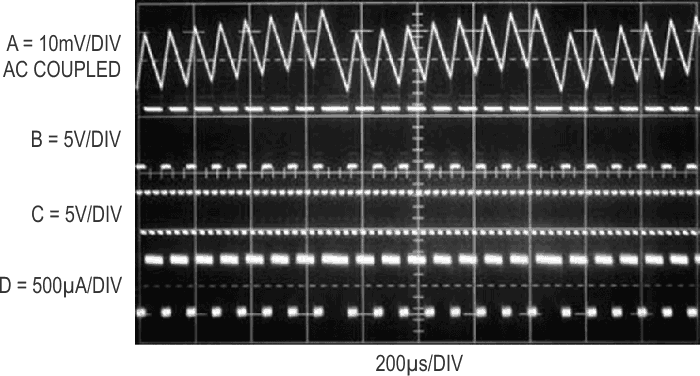
Short term frequency jitter occurs because of the uncertain timing relationship between loop frequency and clock phase. This is normally not a problem because the circuit’s output is usually read over many cycles, e.g., 0.1 to 1 second. Figure 3 shows the effects of the timing uncertainty. Reduced sweep speed allows viewing of phase uncertainty induced modulation of A1’s output ramp (trace A). Note pulse position (traces B and D) irregularity during A1’s major excursions. This behavior causes short term pulse displacement, but output frequency is constant over practical measurement intervals.
 |
|
| Figure 3. | Same trace assignments as Figure 2. Reduced oscilloscope sweep speed shows effect of timing uncertainty between loop and clock. Loop pulse position is occasionally irregular, but frequency is constant over practical measurement intervals |
Circuit linearity is inside 0.0015% (0.15 Hz), gain temperature coefficient is 8 ppm/°C (0.08 Hz/°C) and power supply rejection better than 100 ppm (1 Hz) over a 4 V to 6 V range. The LT1884’s low input bias and drift reduce zero point originated errors to insignificant levels. To trim this circuit, apply 5.0000 V in and adjust the 2 kΩ potentiometer for 10.000 kHz output.
Reference
- Williams, J., “Designs for High Performance Voltage-to-Frequency Converters,” Linear Technology Corporation, Application Note 14.