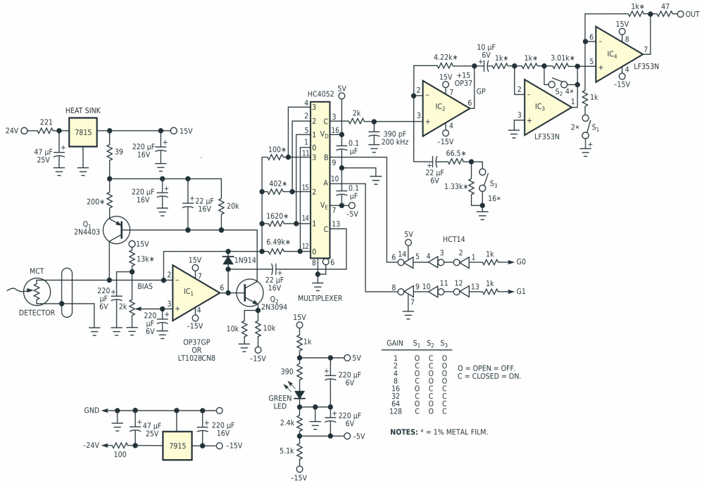
Digitally controlled gain is an everyday analog-design element. You frequently find this element in an op-amp-based, transimpedance current-to-voltage converter. When you design digital gain control into such a converter, the usual scheme is to arrange things such that a digital multiplexer selects the appropriate feedback resistor for each gain figure. In Figure 1, op amp IC1 is connected in a typical topology but with a twist. The normal way to arrange the gain-setting multiplexer would be to take the converter's output directly from the op amp's output pin (IC1, Pin 6). The trouble with this method is that the on-resistance of the multiplexer would then be effectively in series with the selected feedback resistance. In cases such as this one, in which the feedback resistance ranges as low as a few hundred ohms or less, the resulting gain error can be large. For example, the on-resistance of the HC4052 in Figure 1 can exceed 100 Ω. That figure is equal to that of the lowest gain-setting resistor and, therefore, the source of 100% error. The obvious approach, using larger resistors, works poorly when you need high-frequency performance. The resulting RC delay products can cause frequency peaking, ringing, and, sometimes, outright oscillation.
 |
|
| Figure 1. | In this programmable-gain circuit, the on-resistance of the gain-setting multiplexer plays no role in the determination of gain. |
This Design Idea offers an approach that makes the current-to-voltage converter gain independent of multiplexer resistance. The idea is to use two multiplexers in a force/sense topology such that the output comes from the “force” end of the selected gain resistance, rather than directly from the op amp's output. Assuming that the load presented to the “sense” output is reasonably high, the result is a gain product that is insensitive to on-resistance. The remainder of the circuit surrounding IC1 comprises a high-performance bias and preamplifier circuit for a cryogenic (liquid-nitrogen-cooled), mercury-cadmium-telluride infrared detector. These broadband, photoconductive optical sensors are popular in IR spectrometers. They are particularly popular in Fourier-transform-type spectrometers. Their popularity stems from their low noise, wide optical-wavelength responsivity, and electrical response of faster than 1 MHz.
Notable features of the circuit in Figure 1, besides the force/sense gain-setting topology, include dynamic biasing (via Q1 and Q2) of the MCT detector, 64-to-1 (36-dB) digitally programmable gain, 128-to-1 (42-dB) manual-switch-settable gain, approximately 200-kHz bandpass response, and approximately 700-nV rms input-referred noise of less than 1 nV/√Hz). One trick that helps achieve this noise performance, other than the use of the superquiet LT1028 op amp for IC1, is the cascaded-inverter HCT14 structure. The HCT14s serve no purpose other than to block entry of noise, which might be present on the digital gain-setting lines, into the gain-setting-multiplexer circuitry. Without these inverters, any such digital noise, a common cause of gremlins in high-gain, computer-controlled analog circuitry, could easily become capacitively coupled to the ac signal path.