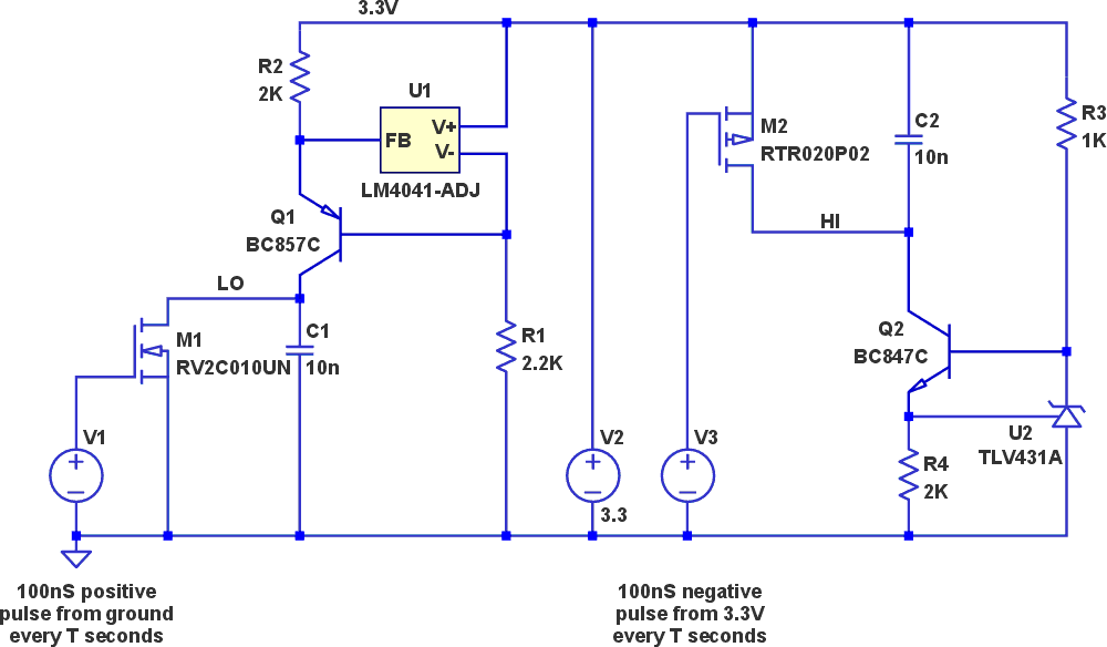
There are multiple means of generating analog sawtooth waveforms. Here’s a method that employs a single supply voltage rail and is not finnicky about passive component values. Figure 1 shows a pair of circuits that use a single 3.3-V supply rail, one producing a ground-referenced sawtooth and the other a supply voltage-referenced one.
 |
|
| Figure 1. | The circuitry to the left of the 3.3 V supply implements a ground-referenced sawtooth labeled “LO”, while that to the right forms a 3.3 V-referenced one labeled “HI”. |
For the LO signal, R1 supplies adequate current to operate U1. This IC enforces a constant voltage VREF between its V+ and FB pins. Q1 is a high beta NPN transistor which passes virtually all of R2’s current (VREF/R2) through its collector to charge C1 with a constant current, producing the linear ramp portion of this ground-referenced sawtooth. (U1’s FB current is typically less than 100 nA over temperature.) M1 is a MOSFET that is activated for 100 ns every T seconds to rapidly discharge C1 to ground. Its “on” resistance is less than 1 Ω and so yields a discharge that lasts more than 10 time constants.
The sawtooth’s peak amplitude A is
where VREF for U1 is 1.225 V. For a 3.3-V rail, the amplitude (A) should be less than an AMAX of 2.1 V, which requires T to be less than
With the availability of a U1 VREF tolerance of 0.2% and a 0.1% tolerance for R2, the circuit’s overall amplitude tolerance is mostly limited by an at best 1% C1 combined with the parasitic capacitance of.
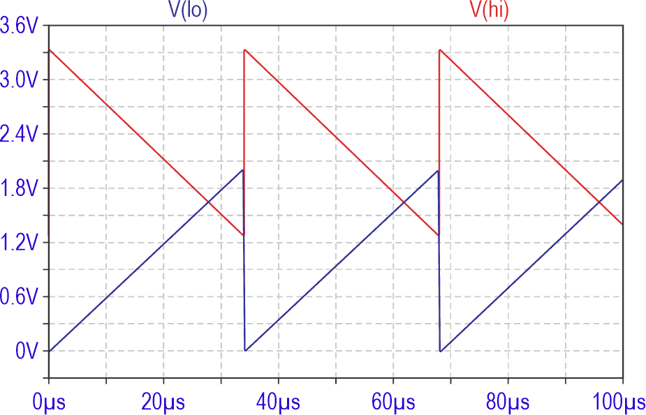
M2, C2, Q2, R3, R4 and U2 work much like the circuit just described, except that they produce an “upside-down” 3.3-V supply-referenced sawtooth. Both waveforms can be seen in Figure 2. With the exception of U2, the tolerance contributions of these components are those previously mentioned for the “right side-up” design respectively. U2’s reference current is typically less than 250 nA over temperature, but its VREF of 1.24 V has at best a 1% tolerance. Figure 2 depicts both sawtooth waveforms.
 |
|
| Figure 2. | The waveforms shown have peak values which are slightly less than the largest recommended. The period T is 34 µs. |
These circuits do not require any precision or matched-value passive components. And there is no need to coordinate these component values with any active component’s parametric values or with the switching period T, as long as T is kept less than TMAX. The only effect that the non-zero tolerances of the passive components and of certain active parameters has been on the peak-to-peak amplitude of the sawtooth waveforms.