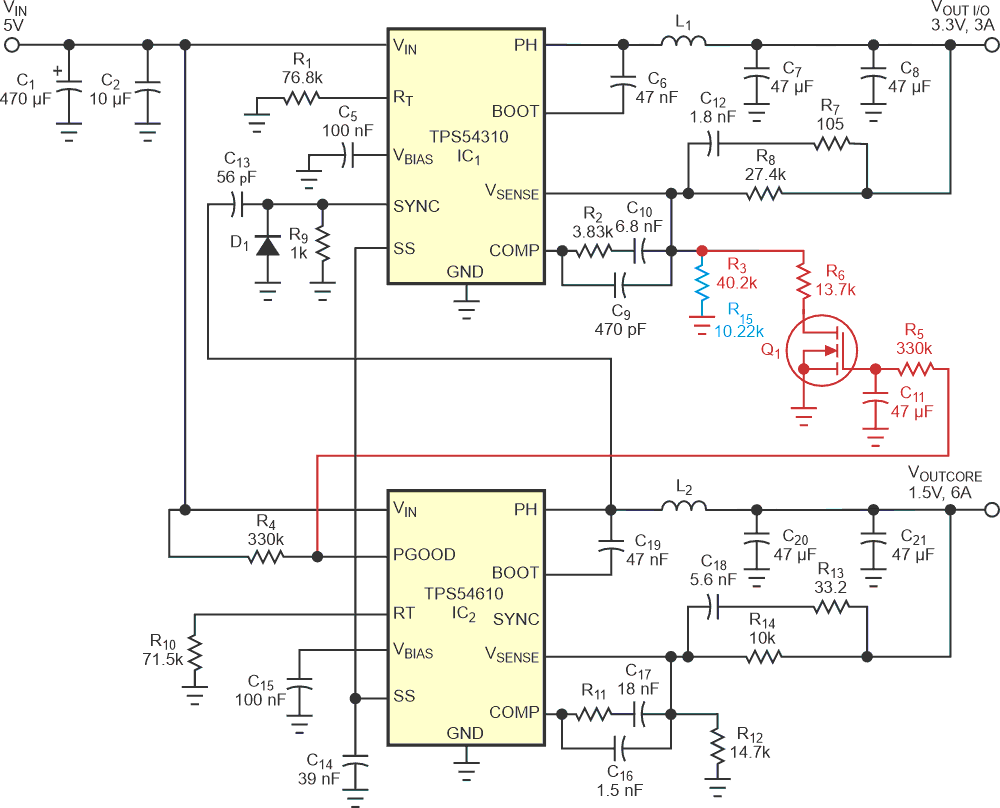
Many applications use FPGAs, ASICs, or DSP chips, which usually require multiple voltage rails, typically two: the core voltage and the I/O voltage. The core voltage is usually lower than the I/O voltage. Guidelines for determining how to power up two or more voltage rails depend on the part and the manufacturer you use. The first implementation in Figure 1 shows how to realize ratiometric sequencing, which means that both power-supply output rails simultaneously start and simultaneously reach their final regulated output voltage. This implementation uses resistor R15 connected to ground; the path and components in red are deleted. You can achieve the ratiometric function by stacking together multiple converters that share one soft-start capacitor. This connection ensures that both controllers ramp up their output voltage at the same time during power-up. Both the IC1 and IC2 controllers share a soft-start capacitor, C14. This example uses two buck converters with integrated synchronous-rectification FETs. From a 5 V input-voltage rail, IC1 generates the 3.3 V I/O voltage. Buck converter IC2 generates the 1.5 V output voltage.
 |
|
| Figure 1. | This circuit provides ratiometric (delete red path and components) or simultaneous power-up sequencing. |
The soft-start pin, available on both controller ICs, serves two purposes. You can use it to enable the controller circuitry if required – an implementation you could realize by tying an open-collector or open-drain gate to the SS Pin. If the transistor or FET is active, it ties the SS Pin to ground potential, forcing both controllers to stay off. Once you release the SS Pin, both ICs start to charge C14 with their internal 5-µA current sources. In total, 10-µA current flows into C14. Once C14 reaches the threshold voltage of 1.2 V, both controllers start to operate. You can easily calculate the delay versus the capacitor's value: Delay time =
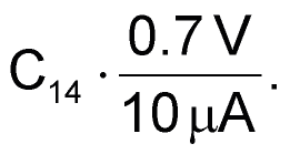
As the output activates, a brief ramp-up at the internal soft-start ramp may occur before the external soft-start rate takes control. The output then rises at a rate proportional to the soft-start capacitor. You can program the soft-start time via C14. The next equation represents the soft-start time calculation. The actual soft-start time is likely to be less than the calculated approximation because of the brief ramp-up at the internal rate. Soft-start time=
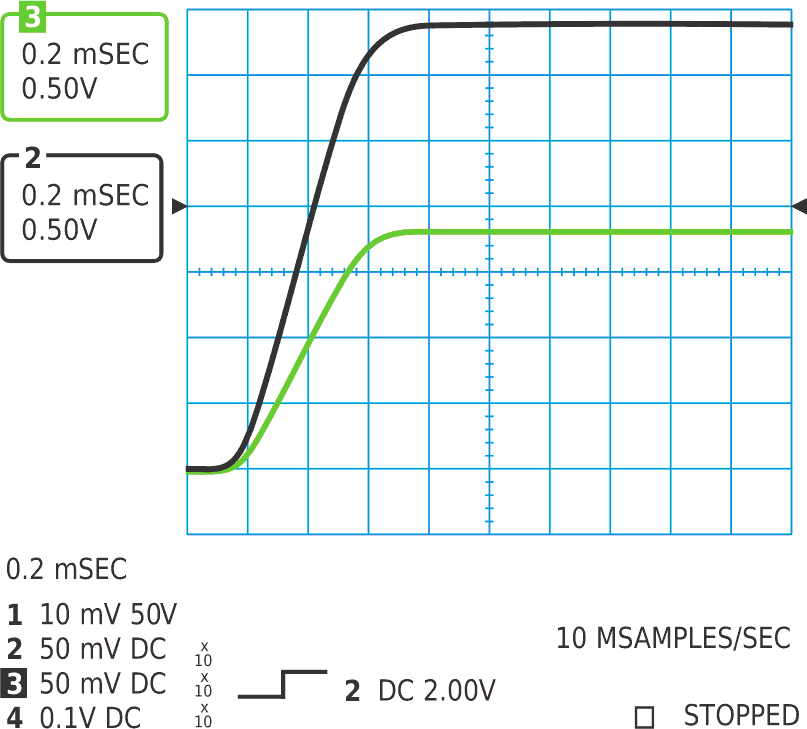
If you set IC1 for 3.3 V and IC2 for 1.5 V, they both reach their final voltage level at the same time. Figure 2 shows measured results of the ratiometric sequencing.
 |
|
| Figure 2. | This graphic shows measurement results for the ratiometric implementation. |
In the simultaneous-sequencing scenario, IC2 acts as the master controller. You program its output voltage via R14 and R12 to a value of 1.5 V. R8 and R3 program the slave controller IC1’s output voltage to a value of 1.5 V. As the ratiometric scenario describes, both voltages start at the same time with the same ramp, reaching their final value at the same time. Once both rails reach 1.5 V, you must increase IC1’s output voltage to 3.3 V, its final value. To make that increase happen, Q1 places R6 in parallel with R3. You can calculate the value of R6 using the next three equations. The given parameters are: VOUTCORE = 1.5 V; R8 = 27.4 kΩ; VREF = 0.891 V, the internal bandgap-reference voltage of IC1; and R3 = 40.2 kΩ. You can program VOUTI/O via R8 and RX. RX represents the value of R3 and R6 in a parallel connection.
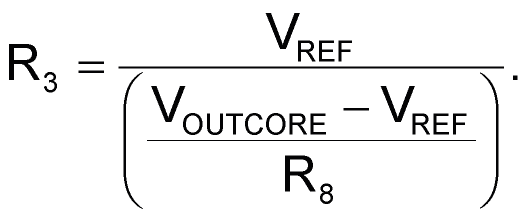
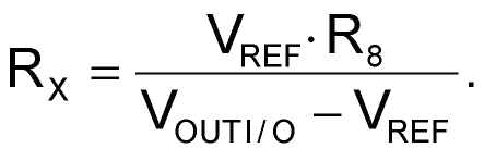
RX must have a value of 10.22 kΩ to produce VOUTI/O = 3.3 V.
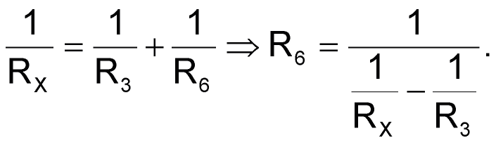
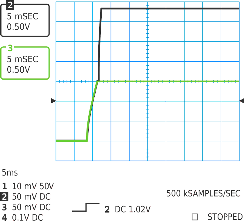
In this example, R6 needs a value of 13.7 kΩ. Applying 5 V to the input-voltage rail activates both controllers at once, allowing them to start at the same time. Once the master controller, IC2, reaches an output voltage level equal to or greater than 90% of the initial value, the IC releases the power-good open-drain-comparator output pin. This action forces the pin to rise immediately to the output-voltage level because of resistor R4’s pullup action. A lowpass filter consisting of R5 and C11 forms a delay circuit, driving MOSFET transistor Q1’s gate. This delay circuitry determines when Q1 becomes active. Q1 has a threshold voltage, VGSTH, of 1.6 V. Once the gate voltage reaches or exceeds the threshold voltage, VGSTH, Q1 starts to conduct, putting R6 in parallel with R3. Because of the resistor-ratio change, IC1’s output voltage ramps up to its final I/O-voltage value of 3.3 V. The MOSFET this design uses has an on-resistance of roughly 10 Ω. This figure might sound high, but, because of the high-ohmic-resistive divider, this value does not affect performance. Figure 3 shows the results of the described implementation during power-up.
 |
|
| Figure 3. | These curves, distinctly different from those in Figure 2, show simultaneous-sequencing results. |
Significantly, in this implementation both converters run at the same switching frequency. IC2 is the master controller, programmed to a 700-kHz switching frequency. IC1 starts at a lower initial switching frequency of roughly 630 kHz, 10% below the switching frequency of IC2. Once IC2 begins to operate, it synchronizes IC1 via the Sync Pin. Diode D1 limits negative voltage spikes at the Sync input. Placing a well-chosen Schottky diode between both output voltage rails can ensure that, even during power-down, both rails have a voltage difference of 400 to 600 mV for safety reasons. The cathode connects to the I/O-voltage rail, and the anode connects to the core rail.