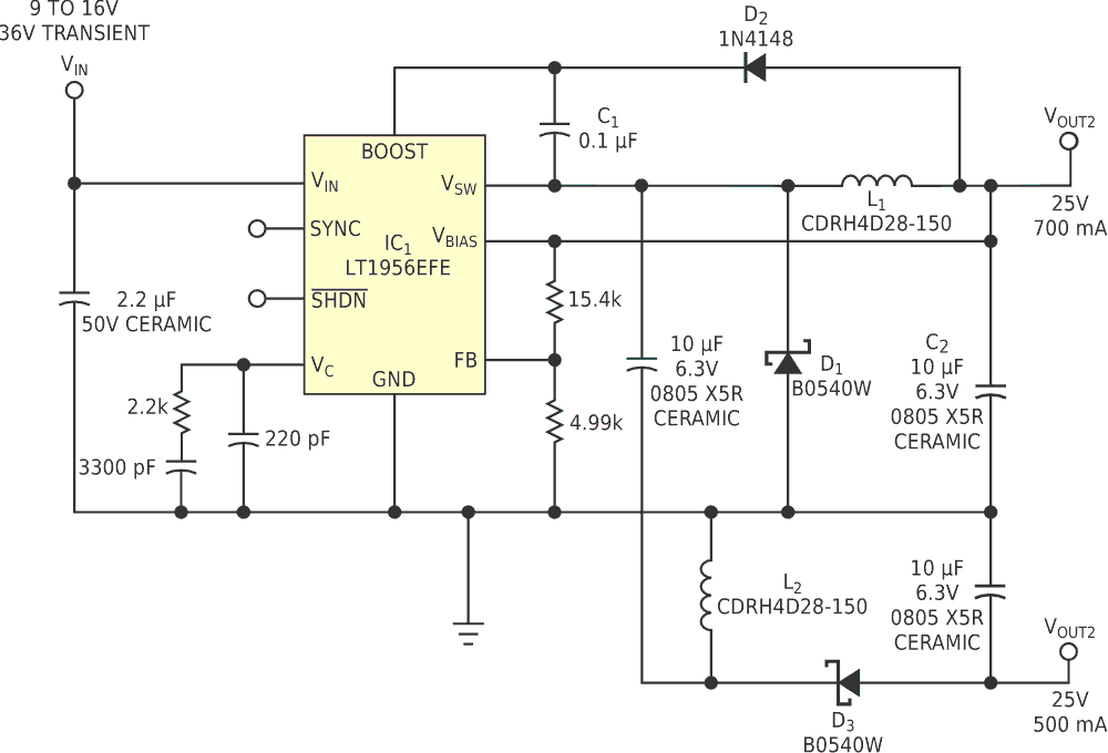
A common problem for power-supply designers is to create a compact, dual-polarity step-down converter. If space and cost are not concerns, the obvious solution is a pair of DC/DC converters, one for each output. But space and cost are almost always issues for communications, data-acquisition, and disk-drive applications. Figure 1 shows a single current-control- regulator approach that supplies 5 V at 700 mA and –5 V at 500 mA from a 12 V system source. The circuit features efficiency similar to that of a two-regulator solution and has no component measuring more than 3 mm high. The low profile and low board real estate that this design requires are almost impossible to match using a flyback design or a similar dual-output SEPIC design using a transformer instead of two inductors. Note, however, one important limitation of this circuit that makes it inappropriate for some applications:
 |
|
| Figure 1. | This dual-polarity DC/DC converter uses a single-switch buck regulator. |
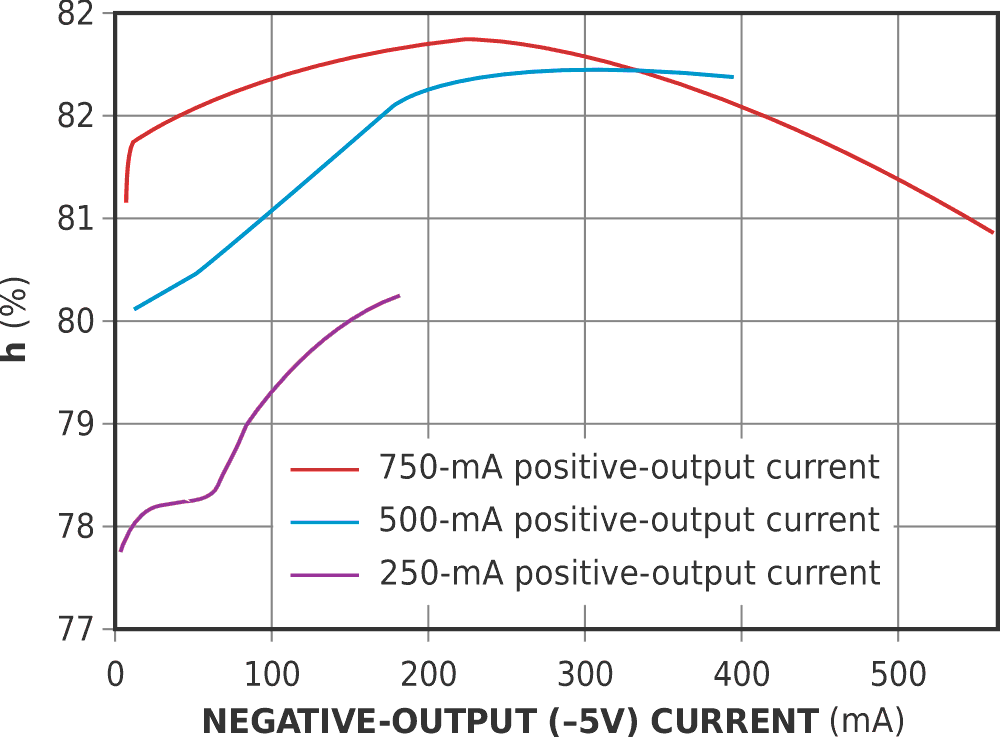
For the circuit to maintain regulation, the positive load must always outweigh the negative load. Figure 2 shows some efficiency curves at various positive-output currents.
 |
|
| Figure 2. | These curves represent efficiency figures for various positive and negative output currents. |
The dual-polarity output circuit is similar to that of a typical single-output positive buck regulator. The circuit adds a secondary negative output by attaching a coupling capacitor (C1), a second inductor (L2), a catch diode (D3), and an output capacitor (C2). The negative output voltage maintains regulation based on the voltage of the coupling capacitor's remaining constant and equal to the 5 V output voltage. Current ramps up and down in the secondary inductor, L2, with the same peak-to-peak ripple as that of the primary inductor, L1. The low-impedance path of the coupling capacitor provides the current to L2 during the on-time of the switch and induces the same voltage across L2 as appears across L1. The Schottky catch diode, D3, provides a current path for the inductor during the off-time of the switch and a current path from the coupling capacitor when discharging into the positive output. Current must flow from the coupling capacitor into L1 during the off-time of the switch for the capacitor to discharge all the charge gained during the on-time of the switch. This current flowing into the positive inductor during the off-time takes the place of some of the current that would normally be sourced from the positive catch diode, D1, reducing the losses in D1 but increasing the losses in D3.
 |
|
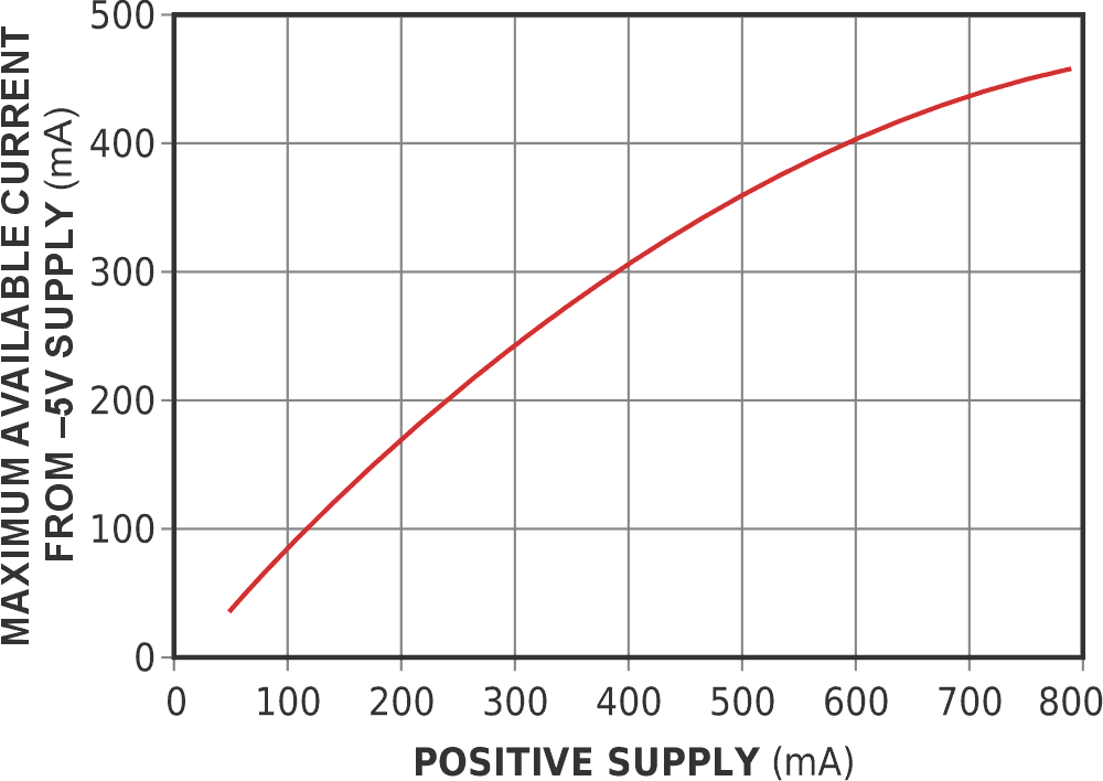
| Figure 3. | This curve gives the maximum available negative-output current as a function of positive-supply current. |
The need for the coupling capacitor to charge and discharge equally creates an important limitation of the circuit: To maintain regulation on both outputs, the negative-supply output current must always be less than the positive-supply output current (Figure 3). If the negative-supply output current increases enough to equal the positive-supply output current, regardless of how great the positive current is, the output voltage begins to collapse. Also, if the negative-supply output current is too low (below 5 to 25 mA, depending on input voltage), the negative-supply voltage can balloon. With extremely light negative loads, the coupling-capacitor discharge current during switch off-time and the inductor current (L2) during switch on-time come only from the negative output capacitor, C2 (as opposed to both the negative output capacitor and the negative dc load). Thus, the output capacitor charges well past its intended voltage because no negative dc load is available to discharge the capacitor. If you use this circuit in an application in which the negative output will see light loads, use a 25-mA preload to maintain regulation.