Analog topologies abound for converting current to voltage, voltage to current, voltage to frequency, and frequency to voltage, among other conversions.
Figure 1 joins the flock while singing a somewhat different tune. This current, voltage, and power (IVW) DC power converter multiplies current by voltage to sense wattage. Here’s how it gets off the ground.
 |
|
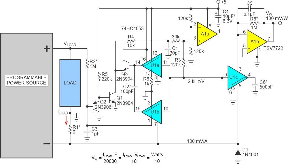
| Figure 1. | The “I×V = W” converter comprises voltage-to-frequency conversion (U1ab & A1a) with frequency (F) of 2000 × VLOAD, followed by frequency-to-voltage, VW, conversion where VLOAD < 33 V and ILOAD < 1.5 A. |
The basic topology of the IVW converter comprises a voltage-to-frequency converter (VFC) cascaded with a frequency-to-voltage converter (FVC). U1ab and A1a, combined with the surrounding discretes (Q1, Q2, Q3, etc.), make a VFC similar to the one described in this previous Design Idea, “Voltage inverter design idea transmogrifies into a 1 MHz VFC” (Ref. 1).
The U1ab, A1a, C2, etc., VFC forms an inverting charge pump feedback loop that actively balances the 1 µA/V current through R2. Each cycle of the VFC deposits a charge of 5 V × C2, or 500 picocoulombs (pC), onto integrator capacitor C3 to produce an F of 2 kHz × VLOAD (= 1 µA / 500 pC) for the control signal input of the FVC switch U1c.
The other input to the U1c FVC is the -100 mV/A current-sense signal from R1. This combo forces U1c to pump

into the input of the A1b inverting integrator.
The melodious result is:

or,

The R6C5 = 100-ms integrator time constant provides >60-dB of ripple attenuation for VLOAD > 1-V and a low noise 0- to 5-V output suitable for consumption by a typical 8- to 10-bit resolution ADC input. Diode D1 provides fire insurance for U1 in case VLOAD gets shorted to ground.
Reference
- Woodward, Stephen. "Voltage inverter design idea transmogrifies into a 1MHz VFC."