The isolated AC-to-DC flyback converter is the most commonly used power supply type for home and industrial devices. Fear of the main voltage and complexity of calculations cause electronic beginners and enthusiasts to procrastinate DIY such circuits. This project introduces an AC-to-DC flyback switching power supply that converts universal 50 Hz AC input (85 V-260 VAC) to 12 VDC-0.5 A (6 W) using the minimum components in the BOM, both price and quantity.
The transformer’s ferrite core is RM6 and DK106 is the controller chip. The inductance of the primary winding of the transformer is 2 mH and the switching frequency is 65 kHz. Output regulation is done through a Zener diode, and the controller chip does not need any external supply rail or an auxiliary winding on the transformer; making it a beginner-friendly DIY circuit to learn and experience.
CAD Software: Altium Designer – Test Equipment: Siglent SDL1020X-E DC Load, Siglent SDS2102X Plus DSO, VEVOR SC240M Thermal Imaging Camera
Circuit analysis
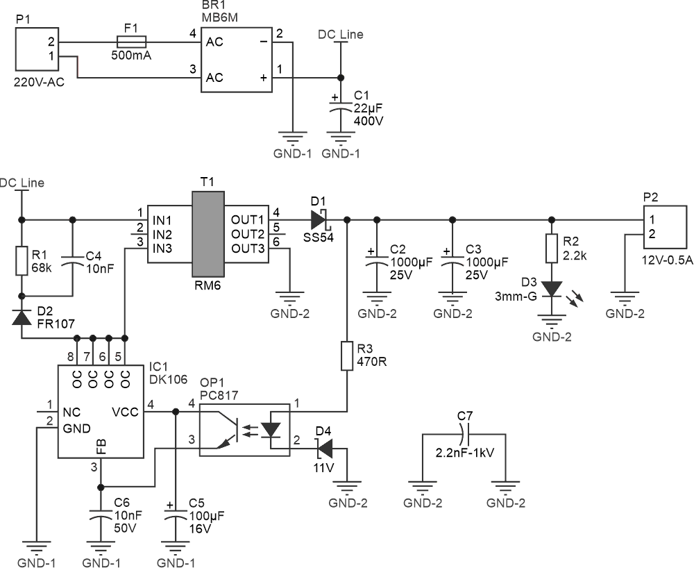
Figure 1 shows the schematic diagram of the device. The heart of the circuit is the controller chip, DK106, which makes it simple, cheap, and easy to build.
 |
|
| Figure 1. | Schematic diagram of the 85 VAC-260 VAC to 12 V-0.5 A AC-to-DC Isolated Flyback Converter. |
According to the datasheet, the features of the DK106 are as follows:
- 85 V – 265 V wide-range AC power input.
- Double chip design with bipolar junction transistor (BJT) to save cost.
- Large-scale MOS digital circuit design with E class BJT driving, so that to enhance its high voltage resistance capability.
- Self-power supply circuit design, no need for additional IC to supply electricity to reduce component and cost.
- Internal integrated constant high voltage current driving circuit, no need for additional resistance.
- Over-current, overloading, over-temperature, over-voltage, output short circuit, and photo-coupler failure protection.
- Internal ramp compensation circuit to keep the stability of the circuit in low voltage and high-power conditions.
- Internal PMW oscillation circuit with Frequency jittering control to keep EMC characteristics.
- Internal frequency conversion. frequency-down in low load conditions complies with the European standard (standby power <0.3 W); also reduces the output voltage ripple.
- Ramp current drive circuit included to reduce IC power loss and raise circuit efficiency.
- 4 kV anti-static ESD test.
P1 is a KF127 terminal for the AC input. F1 is a 500 mA fuse. It is preferred to use a fusible resistor instead of F1 because it helps to reduce the input even further (an RC filter). BR is an MB6M bridge rectifier and C1 is a 22 µF-400 V electrolytic capacitor for ripple reduction. R1, C4, and D2 build an RCD snubber circuit to dampen HV switching spikes and ringing on the Drain pin of the controller’s internal MOSFET (OC pin). C5 and C6 are used for noise reduction.
OP1 is a PC817 optocoupler that provides a galvanically isolated circuit path for the controller to sense the output voltage and adjust the PWM pulse duty cycle at the transformer’s primary. D4 is an 11 V Zener diode to regulate the output voltage level and R3 limits the current to OP1. C2 and C3 are output capacitors for noise reduction and stabilization. D3 is a 3 mm LED, indicating a correct voltage level at the output.
PCB layout
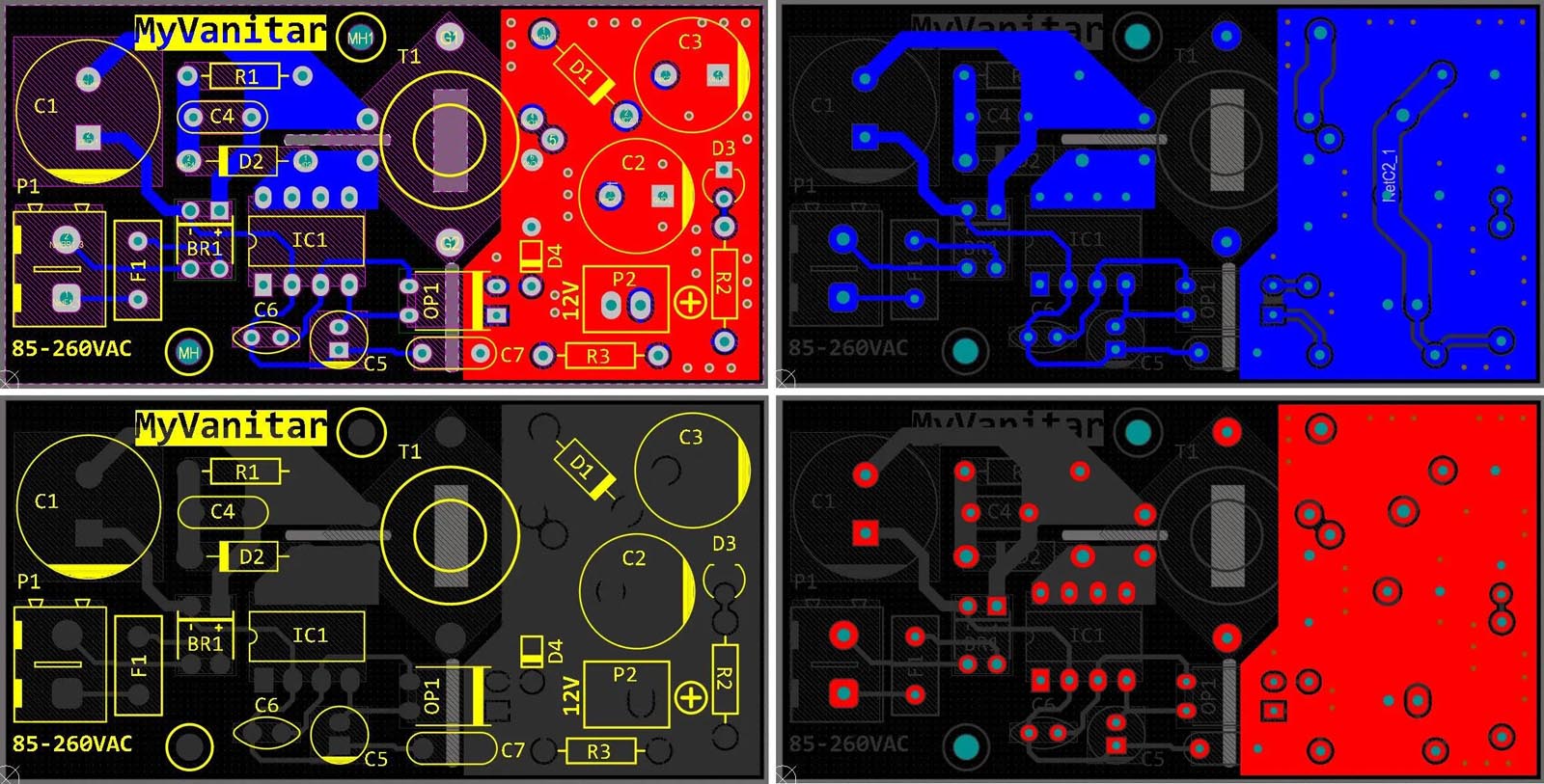
Figure 2 shows the PCB layout of the power supply. It’s a two-layer PCB board and component packages are through-hole; making it easy to solder and build.
 |
|
| Figure 2. | PCB layout of the 85 VAC-260 VAC to 12 V-0. 5A AC-to-DC Isolated Flyback Converter. |
Three isolation gaps (creepage areas) on the PCB are to follow HV IPC standards. Two stitched polygon pours at the output reduce the length and impedance of the ground path; the result is lower noise and EMI. For the same purpose, the drain pin of the MOSFET (OC pin of the controller chip) must be as close as possible to the primary winding of the transformer. Also, the snubber circuit should be placed as close as possible to the transformer, and loop areas should be minimized. Figure 3 shows the assembly drawing.
 |
|
| Figure 3. | Assembly drawing. |
Assembly
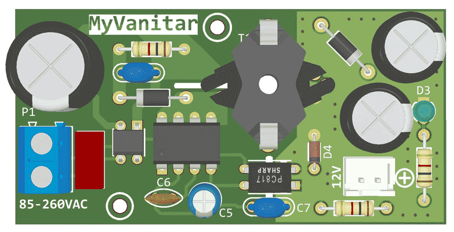
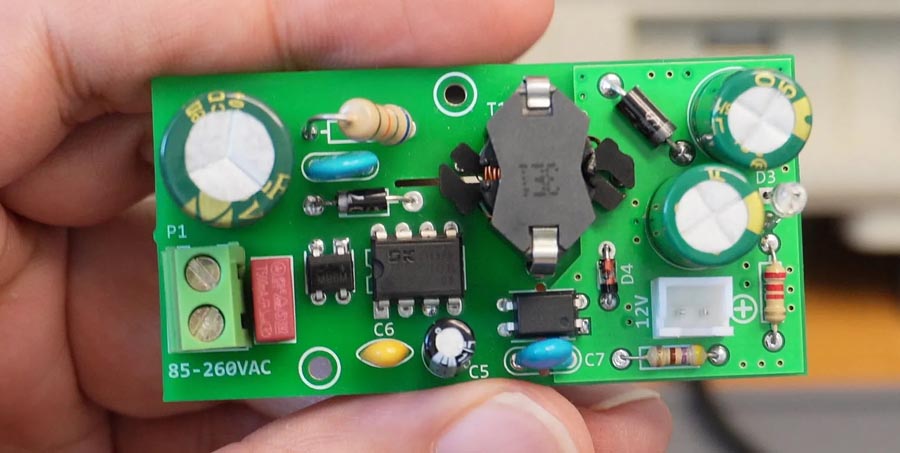
Figure 4 shows the assembled PCB board, you shouldn’t have any problem with soldering the components using an ordinary soldering iron. Clean PCB flux residues using 99% isopropyl alcohol, especially where is close to the high-voltage components. Flux residues can cause short circuits and instability.
 |
|
| Figure 4. | Assembled PCB board. |
Transformer
Figure 5 shows the winding pattern of the transformer. The ferrite core is RM6.
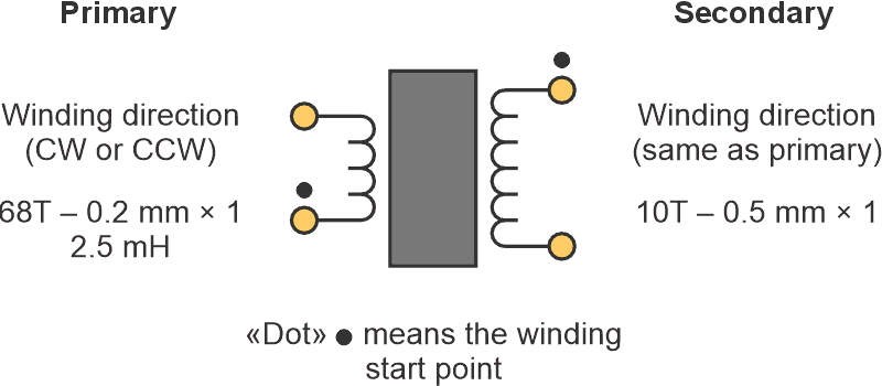 |
|
| Figure 5. | Transformer and winding directions. |
Start the procedure by winding the primary, clockwise or counterclockwise. Then put the ferrite cores in place (in the bobbin) and measure the inductance of the primary winding using an LCR meter. If you can set the measurement frequency on your LCR meter, the best frequency is 65 kHz (switching frequency of the transformer), otherwise, set it to 40 kHz. Grind the middle leg of the ferrite core and measure the inductance of the primary winding till you measure a value as close as possible to 2.5 mH. A small tolerance is acceptable and does not cause a problem (for example 2.46 mH or 2.54 mH). Finally, wind the secondary and put the transformer in place.
Test
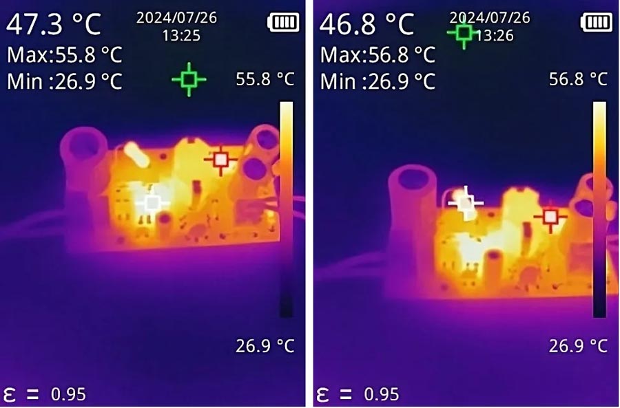 |
|
| Figure 6. | Thermal stress of the components (500 mA load for 15 min), Input Voltage: 220 VAC. |
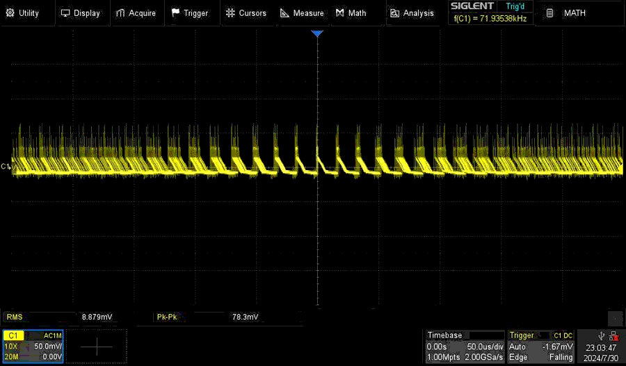
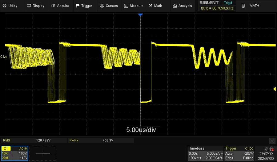
This power supply has been tested for output voltage stability (using Siglent SDL1020 DC Load), output noise (using Siglent SDS2102X Plus DSO), and thermal stress (VEVOR SC240M). The PWM waveform on the OC pin of the controller (Drain pin of the internal MOSFET) was monitored for stability, HV spikes, and ringing to examine the effectiveness of the snubber. Figure 6 shows the thermal stress on the components after 15 minutes of maximum continuous workload. The hottest point was spotted on the output Schottky diode (around 56 degrees C), the controller temperature was measured at around 47 degrees C, and the snubber resistor was also measured at around 47 degrees C (ambient temperature was around 27 degrees C). Figure 7 shows the output voltage stability and Figure 8 shows the output noise (maximum). Figure 9 shows the waveform of the OC pin (input ground referenced). It depicts a close-to-ideal instance of damping the HV spikes and ringing.
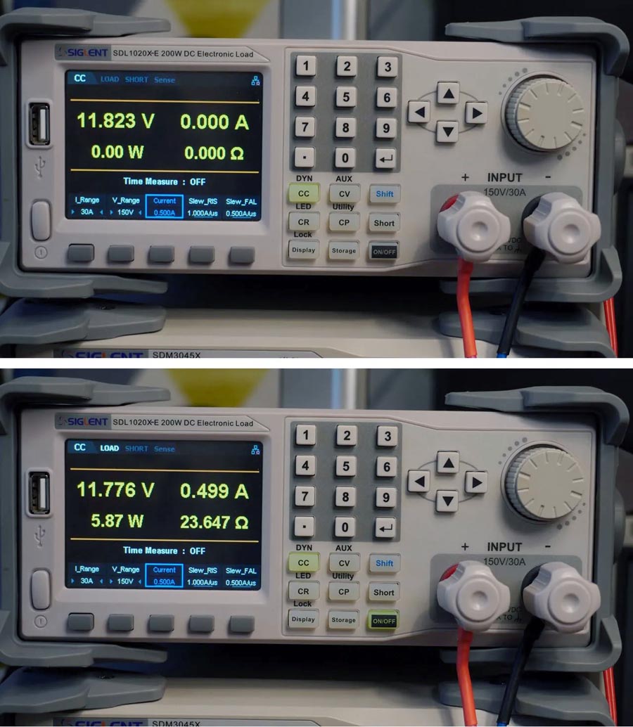 |
|
| Figure 7. | Output voltage stability load regulation (no load, 0.5 A load). |
 |
|
| Figure 8. | Power supply output noise (500 mA load). |
 |
|
| Figure 9. | OC pin waveform (input ground referenced). |
More Improvements
Using an RC snubber in parallel with the output Schottky diode can further reduce the EMI (R = 10R-0.5 W, C = 1 nF-100 V). Using a 10R-1 A fusible resistor instead of F1 acts as an RC filter and helps to reduce the high-frequency AC input noise.