This project features a compact and efficient DC-DC buck-boost converter, based on the XL6019 chip, designed to maintain a stable 12 V output over a wide input voltage range of 9 V to 30 V. The XL6019 is a high-performance switching regulator capable of operating in buck (step-down) and boost (step-up) modes, making it ideal for applications where the input voltage may vary above or below the desired output voltage (such as in cars and trucks). The circuit can deliver up to 2 A of output current when a heatsink is installed on the chip to manage heat dissipation. This converter design, featuring a bifilar-wound common-mode choke with the XL6019 chip, is very likely being shared online for the first time.
Circuit analysis
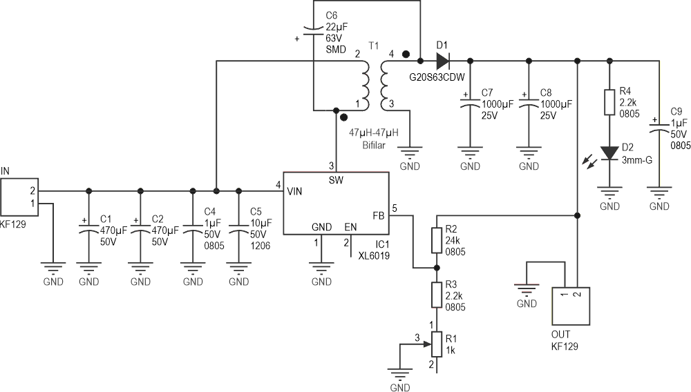
Figure 1 shows the schematic diagram of the converter. IC1 is the heart of the circuit that includes a 5 A NDMOS switch.
 |
|
| Figure 1. | Schematic diagram of the XL6019 buck-boost converter. |
According to the datasheet, the XL6019 is a high-performance DC-DC converter chip that can work in boost, buck-boost, or inverting configurations. It supports both positive and negative output voltages and operates over a wide input voltage range from 5 V to 40 V.
It uses current-mode control to improve response during voltage changes and operates at a fixed switching frequency of 180 kHz. The chip integrates a powerful N-channel MOSFET that can handle up to 5 A of switching current, making it suitable for medium-power applications.
The XL6019 includes several built-in features for reliable operation:
- Soft-start function to reduce inrush current at power-up
- Over-voltage protection on the switch pin
- Current limit and thermal shutdown protections
- High efficiency, up to 94% under typical conditions
- Enable pin for easy on/off control using logic-level signals
It is available in a TO-263-5L package, making it easy to mount on standard PCBs with proper heatsinking.
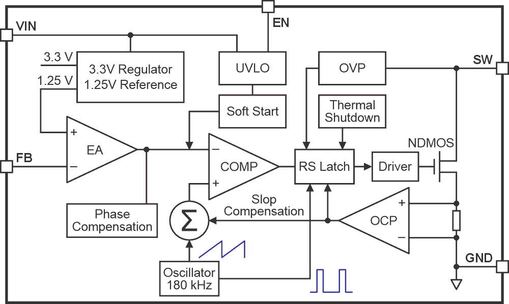
This chip is ideal for automotive, industrial, and portable electronic applications that require a stable output voltage despite input voltage variations. Figure 2 shows the functional block diagram of the chip.
 |
|
| Figure 2. | Functional block diagram of the XL6019. |
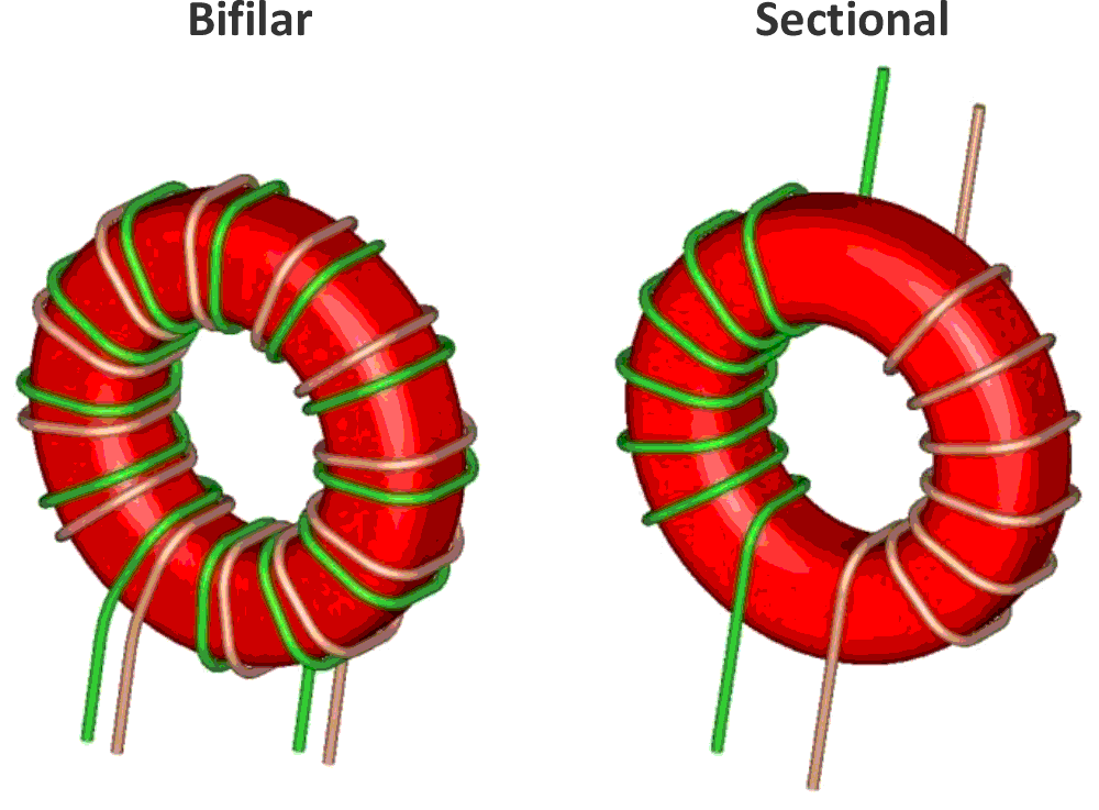
C1 and C2 are large input capacitors for noise reduction and damping the inrush current. The small C4 and C5 capacitors are placed as close as possible to the controller to absorb high-frequency noises. T1 is a bifilar common-mode choke to transfer the energy to the output. Figure 3 shows two types of common-mode chokes (sectional and bifilar).
 |
|
| Figure 3. | Two types of common-mode chokes (sectional and bifilar). |
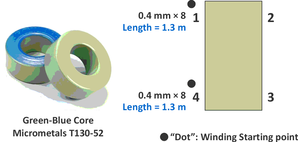
The inductance of each choke’s winding should be around 47 µH to 50 µH. The peak current of the inductor/switch is around 5 A, and the maximum inductor ripple current is around 20%. Selected core type is Micrometal’s T130-52 green-blue iron powder toroid core. Figure 4 should handle all the necessary info to wind the choke.
 |
|
| Figure 4. | The choke core type and winding pattern. |
C7, C8, and C9 are output capacitors used for noise reduction and to stabilize the controller. D2 is a 3 mm LED to indicate the presence of output voltage. R1, R2, and R3 are feedback resistors. R1 can set the output voltage anywhere between 11 V and 13 V.
D1 is a strong 20 A-63 V DPACK Schottky diode to rectify the voltage. The G20S63CDW is a high-efficiency trench Schottky rectifier diode manufactured by Diodes Incorporated. It is designed for applications that require high current handling and low forward voltage drop, making it suitable for power conversion and management circuits.
Key features:
- Maximum repetitive peak reverse voltage: 63 V
- Maximum DC blocking voltage: 63 V
- Average rectified output current: 20 A (at TC = 110 °C)
- Peak forward surge current: 150 A (8.3 ms single half sine-wave)
PCB layout
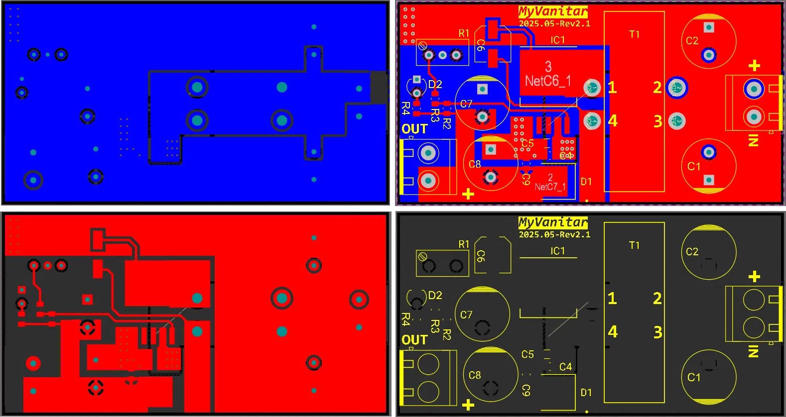
Figure 5 shows the PCB layout. It’s a two-layer PCB board, and I used a mixture of SMD and through-hole components.
 |
|
| Figure 5. | PCB layout of the XL6019 buck-boost converter. |
The ground copper planes on the top and bottom layers are designed to minimize the current path length and impedance. This approach enhances the converter performance and reduces noise and EMI. Additionally, placing the input capacitors (C4 and C5) close to the controller’s input pin is recommended.
Placement of vias is close to critical areas such as the ground pin of the controller and capacitors. It reduces the impedance of the current path and enhances current handling (check vias next to the controller pins).
The switching pin of the controller (Pin 3) is as close as possible to the inductor. Because the copper plane between the controller’s Pin-3 and the inductor’s Pin-1 contains wild switching currents, it could easily act as an antenna and cause higher-than-standard radiated emissions.
“Thermal relief” is a method of connecting the heat-sensitive components (such as the capacitor pins) to the copper plane next to a heat source. That’s why I’ve implemented thermal relief for C7, C8, and C9, which share the same copper plane as the Schottky diode (heat source). Although the installed Schottky diode is quite robust for this current level and is unlikely to generate significant heat, this precaution improves thermal management. High temperature dramatically affects a capacitor’s lifetime; that’s why you notice bulgy capacitors quite often in power supplies.
Assembly and test
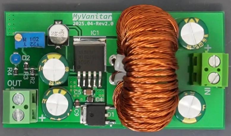
Figure 6 shows the assembled PCB. Soldering this board is easy because the smallest component package size is 0805, and there are no components with low clearance sizes.
 |
|
| Figure 6. | Buck-boost converter assembled board. |
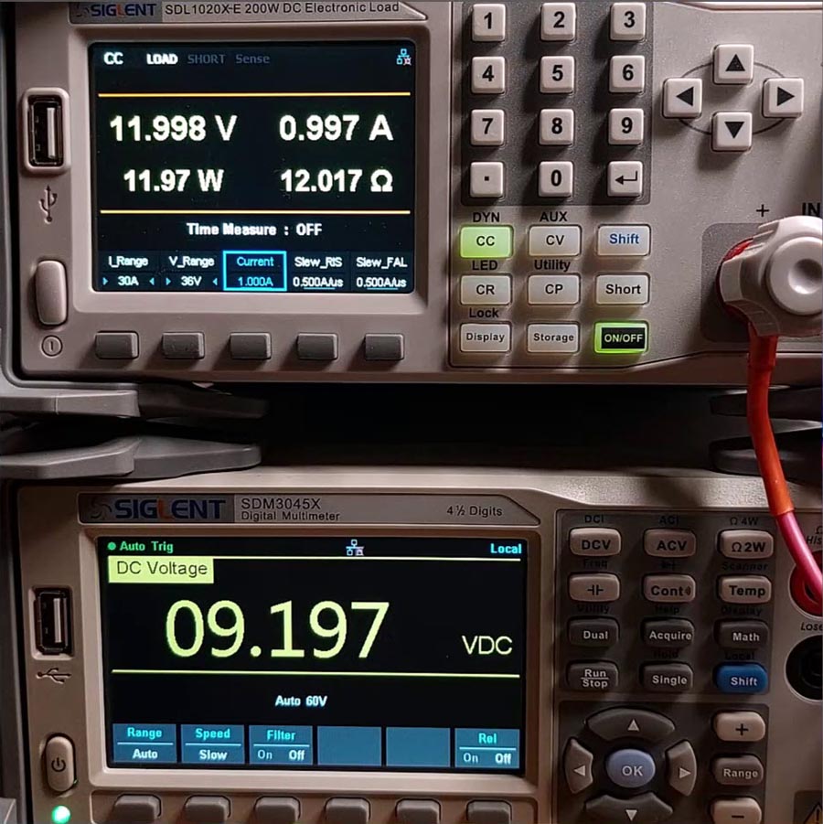
I’ve tested the board within the full input voltage range (9 V to 30 V) using the SDL1020X-E DC load, confirming its voltage stability and current handling (Figure 7).
 |
|
| Figure 7. | Full input voltage range, output stability, and current handling tests. |