Stephen Woodward’s “Ignoring the regulator’s reference” (Ref. 1) Design Ideas (DI) (see Figure 1) is an excellent, working example of how to include a circuit in the feedback loop of an op amp to support the stabilization of the circuit’s operating point. This is also previously seen in “Improve the accuracy of programmable LM317 and LM337-based power sources” (Ref. 2) and numerous other places. I’ll refer to his DI as “the DI” in subsequent text.
 |
|
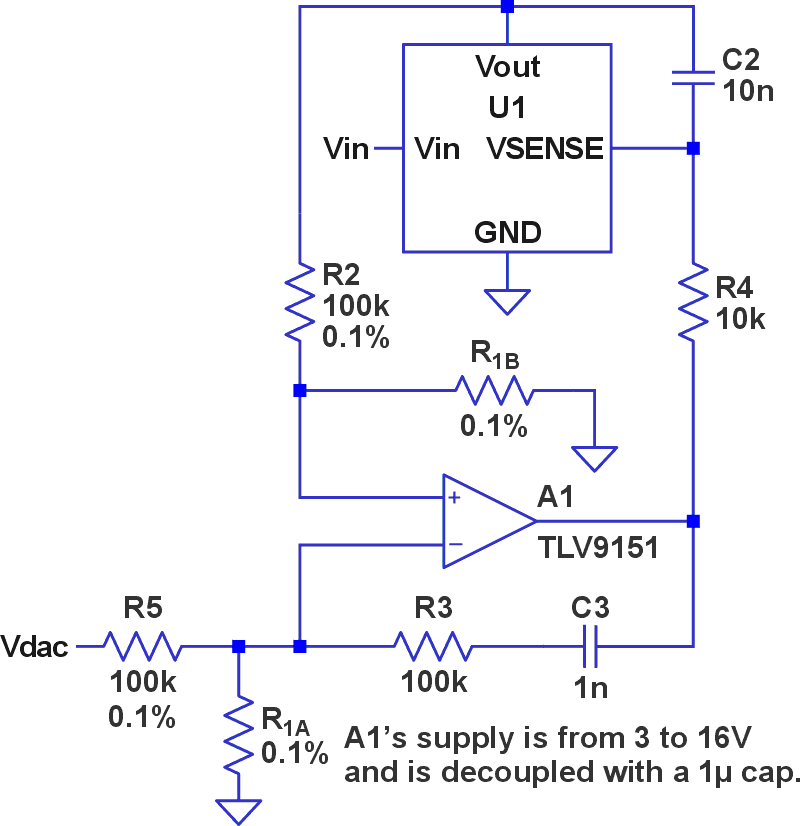
| Figure 1. | The DI’s Figure 1 schematic has been redrawn to emphasize the positioning of the U1 regulator in the A1 op amp’s feedback loop. The VDAC signal controls U1 while ignoring its internal reference voltage. |
A few minor tweaks optimize this circuit’s dynamic performance and leave the design equations and comments in the DI unchanged. Let’s consider the case in which U1’s reference voltage is 0.6 V, VDAC varies from 0 to 3 V, and VOUT varies from 5 to 0 V.
The DI tells us that in this case, R1A is not populated and that R1B is 150k. It also mentions driving Figure 1’s VDAC from the DACOUT signal of Figure 2, also found in “A nice, simple, and reasonably accurate PWM-driven 16-bit DAC” (Ref. 3).
The Figure 2 PWMs could produce a large step change, causing DACOUT and therefore VDAC to quickly change from 0 to 3 V.
 |
|
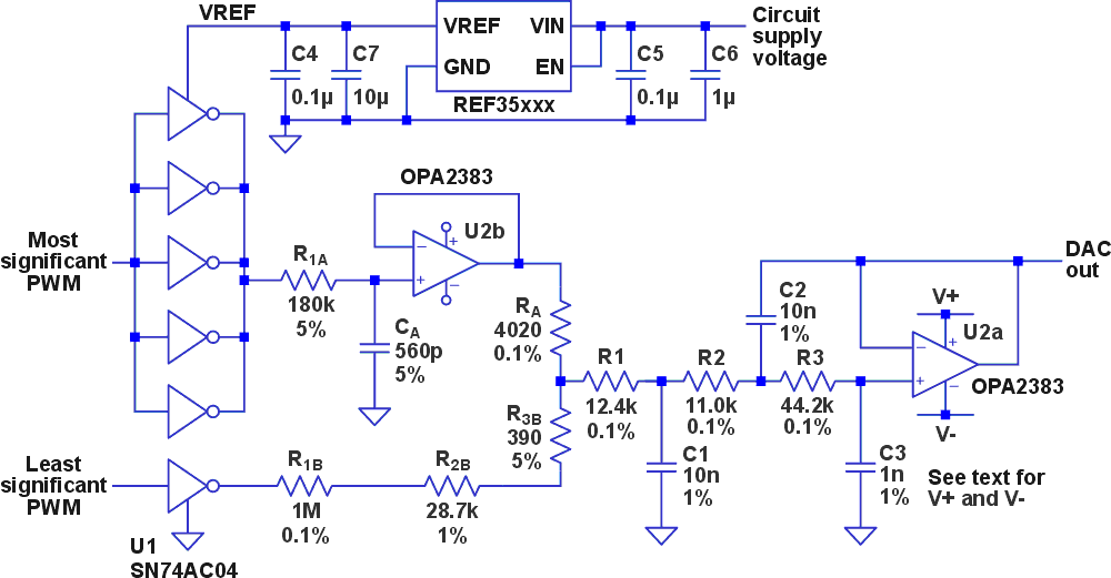
| Figure 2. | Each PWM input is an 8-bit DAC. VREF should be at least 3.0 V to support the SN74AC04 output resistances calculable from its datasheet. CA and C1–C3 are COG/NPO. |
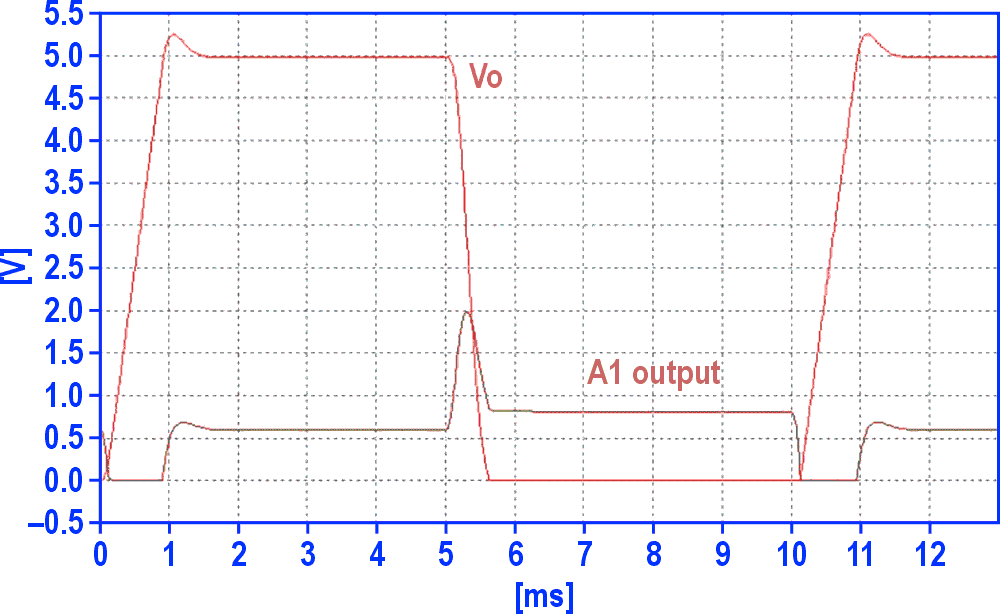
Figure 3 shows how VOUT and the output of A1 react to this while driving a hypothetical U1, which is capable of producing an anomaly-free (Ref. 4) 0-volt output.
 |
|
| Figure 3. | VOUT and A1’s output from Figure 1 react to a step change in VDAC. |
Even though VOUT eventually does what it is supposed to, there are several things not to like about these waveforms. VOUT exhibits an overshoot and would manifest an undershoot if it didn’t clip at the negative rail (ground). The output of A1 also exhibits clipping and overshooting. Why are these things happening?
The answer is that the current flowing through R5 also flows through R3, causing an immediate change in the output voltage of A1. That change causes a proportional current to flow through R4. However, the presence of C2 prevents an immediate change in VOUT and delays compensatory feedback from arriving at A1’s non-inverting input. How can this delay be avoided?
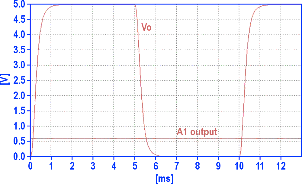
Shorting out R3 makes matters worse. The solution is to remove C2, speeding up the ameliorative feedback. Figure 4 shows the results.
 |
|
| Figure 4. | With C2 eliminated, so are the clipping and the over- and undershoots. The A1 output moves only a few millivolts because of the large DC gain of the regulator, and because it is no longer necessary to charge C2 through R4 in response to an input change. |
VOUT now settles to ½ LSbit of a 16-bit source in 2.5 ms. Changing C3 to 510 pF (10% COG/NPO) reduces that time to 1.4 ms. Smaller values of C3 provide little further advantage.
The VOUT-to-VSENSE feedback becomes mostly resistive above
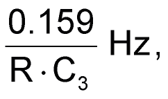
where:
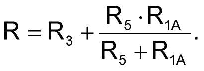
In this case, that’s 1600 Hz, well below the unity gain frequency of pretty much any regulator, and so there should be no stability issues for the overall circuit. Note that A1’s output remains almost exactly equal to the regulator’s reference voltage. This, and the freedom to choose the R5/R1A and R2/R1B ratios, leaves open the option of using an op amp whose inputs and output needn’t approach its positive supply rail.
The (original) DI is a solid design that obtains some dynamic performance benefits from reducing the value of one capacitor and eliminating another.
References
- Woodward, Stephen. "Ignoring the regulator’s reference."
- Paul, Christopher. "Improve the accuracy of programmable LM317 and LM337-based power sources."
- Paul, Christopher. "A nice, simple, and reasonably accurate PWM-driven 16-bit DAC."
- Paul, Christopher. "Enabling a variable output regulator to produce 0 volts? Caveat, designer!"