To test products in my R&D lab, I build many universal data-acquisition systems that connect to a PC or another controller through RS-232 links or LANs. These small systems typically include multiple ADC, DAC, and digital-I/O channels to control various hardware functions during product design and development. Over the years, I have established a simplified analog-interface standard that spans a 0 to 5 V range. On the digital side, many of the newer logic families no longer tolerate 5 V inputs and have rendered 5 V-only digital-I/O ports obsolescent.
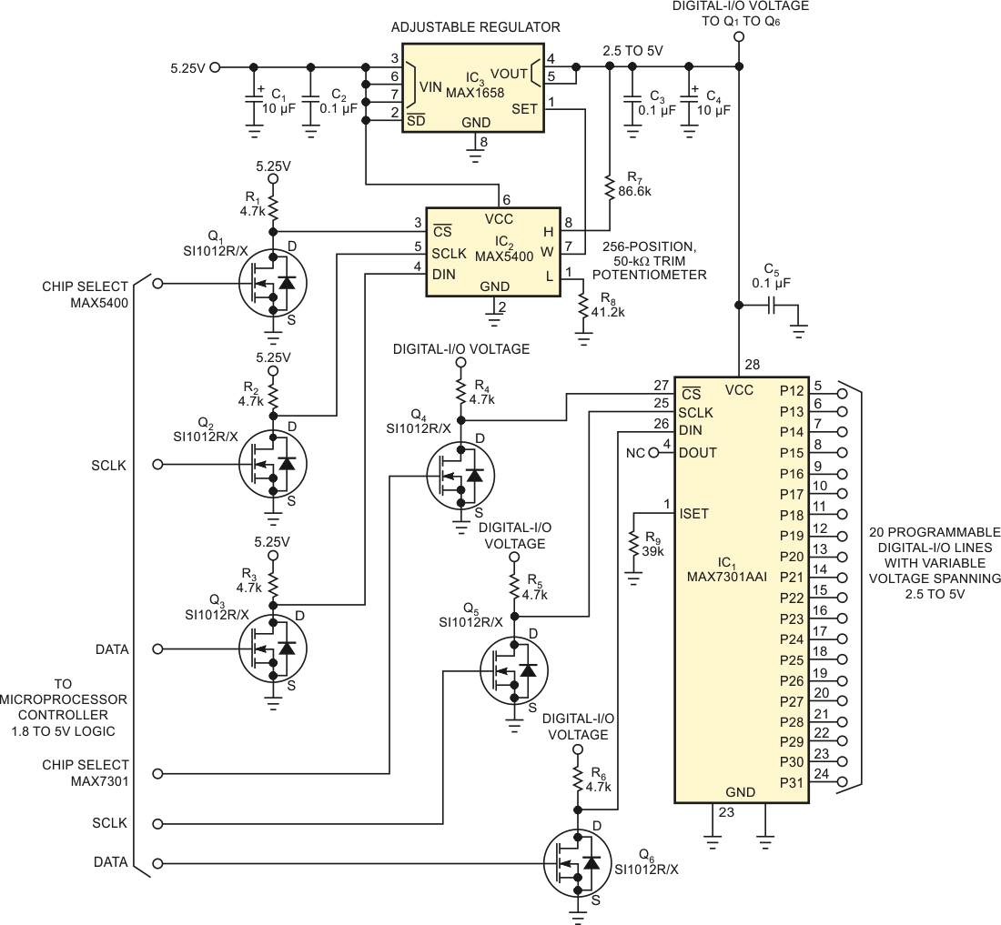
To solve the problem, I designed a flexible digital-interface circuit around a MAX7301 I/O expander from Maxim Integrated Products and a programmable linear-power supply comprising a MAX1658 adjustable linear-voltage regulator under the control of a MAX5400 256-position, digitally programmable potentiometer. This circuit provides a programmable interface matching the logic levels of ICs that require 2.5, 3, 3.3, and 5 V power supplies.
Two SPIs (serial-peripheral interfaces) control all 20 of the MAX7301AAI’s input and output pins and voltage thresholds (Figure 1). Unlike some SPI-port expanders that include weak, resistor-only pullups, the MAX7301, IC1, features true, active-pullup, “totem-pole” outputs that can source higher currents. When powered by the SPI-programmable linear regulator, the MAX7301’s outputs can deliver logic levels of 2.5 to 5 V. The programming interfaces for both devices comprise two three-wire (plus ground) SPI connections that use only six of the controller’s signal lines.
 |
||
| Figure 1. | A programmable power supply sets voltage thresholds for a universal digital-I/O device. | |
Six Vishay Si1012R low-gate-voltage-threshold N-channel MOSFETs, Q1 through Q6, isolate the controllers’ fixed-output-voltage levels from IC1’s variable-input-threshold voltages. Although any of several IC-level-translator ICs work equally well, the inexpensive MOSFET buffers occupy small footprints on the interface’s PCB (printed-circuit board). For operation at serial-interface clock rates approaching IC1’s 26-MHz maximum, optimize the values of resistors R1 through R6 to provide adequate rise times at the selected clock rate. These values are adequate for operation at the 1-MHz SPI clock rate that a low-power microcontroller produces.
To alter the circuit’s output-voltage level, IC2, a 256-step Maxim MAX5400 digital potentiometer, controls IC3, a Maxim MAX1658 adjustable-voltage linear regulator. Writing all zeros to IC2 sets IC3’s output voltage to slightly more than 5 V, and writing all ones (255 decimal) to IC2 reduces IC3’s output voltage to slightly less than 2.5 V. To compensate for component tolerances, the circuit provides enough voltage overrange to cover the full 2.5 to 5 V range. Writing 128 (decimal) to IC2 should produce a nominal 3.25 V output. Measure IC3’s actual output voltage and subtract it from the nominal voltage to produce an offset count for calibration correction.
In operation, the host controller sets IC3’s regulated output voltage through IC2 and determines the maximum voltages of IC1’s logic inputs and outputs. Next, the controller configures IC1’s inputs and outputs as necessary for the interface task at hand. The MAX7301’s standard CMOS logic-threshold voltages of 0.3 to 0.7 times its supply voltage for low and high inputs, respectively, interface with other CMOS parts.