Although an SMPS (switch-mode power supply) can protect itself against permanent short circuits, it sometimes has problems when dealing with transient overloads. Transient overloads are not short circuits but can push the power supply above its nominal load value. This scenario occurs with typical loads such as printer heads and small motors. When facing such a load profile, the power supply can easily trigger its protection circuit, especially if the open-loop gain is high. You will see any decrease in the output voltage on the primary side as a loss of feedback current, because the controller cannot keep the voltage constant.
 |
||
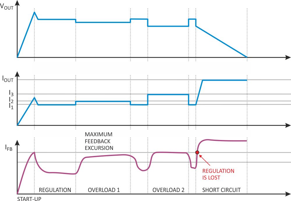
| Figure 1. | Overloads and short circuits can be similar in this typical power profile for a printer. | |
Figure 1 shows a typical power profile for a printer. You can clearly see the power variations and the corresponding feedback-voltage swings that occur. The start-up sequence is a short circuit because, with VOUT far from its target, the feedback current is not yet established. The nominal output current, I1, corresponds to the regulation zone, in which the load is constant. When a first overload occurs (I2 in Figure 1), the feedback pin pushes the primary-current setpoint (in a current-mode controller), but the waveform's excursion starts to diminish, because it is approaching its maximum level. In I3, the power supply has difficulty remaining in regulation and, in short-circuit condition, VOUT collapses to ground. If the primary PWM controller has a simple short-circuit-protection scheme, the protection mechanism can trigger in the overload zones 1 and 2, whereas it should trigger only in the final one. Figure 2 portrays an approach based on the NCP1200 from ON Semiconductor.
 |
||
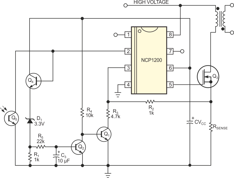
| Figure 2. | A transistor network increases the peak current for a moment until the power supply gives up by reducing the peak setpoint. |
|
This circuit permanently monitors the feedback line (Pin 2) to detect whether a short circuit is present on the secondary side. If so, Pin 2 jumps to its internal pullup voltage and triggers a protective burst mode. Note that this protection acts independently of any badly coupled auxiliary level, because the high-voltage source (Pin 8) directly powers the controller. In the presence of overloads 1 and 2, Pin 2 would jump to the maximum of its capability and would trigger the protection. This circuit does not delay the rise of the feedback voltage but momentarily increases the output-power level by a given percentage. When IOUT is within regulation, Pin 2 is below 3 V and D1 is not biased. As a result, Q2 is blocked and Q1 pulls R3's lower terminal to ground. The current-sense pin therefore sees a current image, which the voltage-divider ratio of R2 and R3 affects.
In this example,

where VSENSE is the voltage across RSENSE. If the NCP1200 imposes a maximum-current setpoint of 1 V, the IC authorizes 1.2 V over RSENSE as long as Q1 is biased (instead of 1 V in a regular configuration). As soon as Pin 2 jumps to a higher value, such as 4 V, indicating a loss of regulation or a severe overload, D1 starts to conduct via Q4. This transistor buffers the feedback-pin impedance: C3 starts to charge up via R5, and, when it reaches approximately 0.7 V at 25 °C, Q1 opens. The divider goes away, the power supply no longer ensures a large peak current, and VOUT goes down, thereby properly triggering the protection. As result, by dimensioning the R5 and C3 elements, you can insert a delay to enable the supply to cope with transient loads.