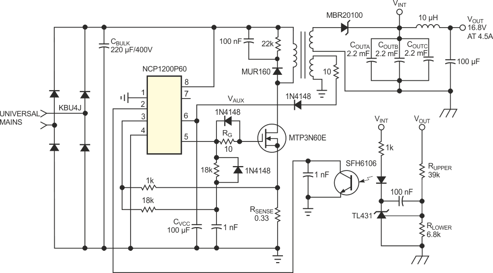
In flyback converters that use primary regulation, the loose coupling between the power secondary and the primary auxiliary windings often results in poor cross-regulation. This situation arises mainly from the leakage inductance but also comes from the level of the primary clamp voltage. Figure 1 shows a typical application schematic using NCP1200 in an auxiliary-winding configuration. This IC uses a DSS (dynamic self-supply), but in some low-standby-power applications, it is desirable to permanently disconnect this feature through an auxiliary level. The DSS simply acts as a standard start-up current source until the auxiliary level takes over.
 |
|
| Figure 1. | In this circuit, leakage inductance in the auxiliary winding can invalidate the controller’s short-circuit-protection circuitry. |
In this application, the regulation takes place on the secondary side by means of the TL431, but the primary level assumes importance in short-circuit conditions. Each time the NCP1200’s VCC crosses 10 V while dropping, the internal logic senses the eventual presence of a short circuit through the feedback pin. Should the circuit confirm a short circuit, the NCP1200 emits a safe-autorecovery, low-frequency burst. However, if poor coupling prevents the auxiliary winding from collapsing, in the presence of a secondary short circuit, VCC never crosses the 10 V threshold, and damage to the circuit may ensue.
 |
|
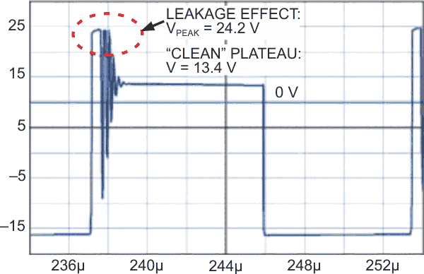
| Figure 2. | The leakage inductance on the auxiliary-winding side causes high rectified voltages. |
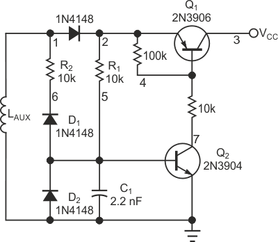
Figure 2 details the effects of the leakage inductance when a short circuit occurs at the output. As you can see, the leakage spike pushes the auxiliary level well above its regular plateau voltage, which is the value you’d like to obtain. With the rectifying diode playing the role of an envelope detector, the result is a final level close to 24 V, far from the 13.4 V you would expect. As a result, a possibly destructive condition exists if the levels exceed the maximum ratings in the controller’s data sheet. You need to clamp the auxiliary voltage using a dissipative element, such as a zener diode. Figure 3 shows the circuitry you adopt to avoid the leakage-inductance problems. The component arrangement actually implements a self-contained sample-and-hold system. When the main power switch is on, capacitor C1 discharges through R2 and D1, and D2 avoids a large reverse bias of Q2’s base-emitter junction. When the main switch opens, the secondary voltage sharply rises, and Node 1 becomes positive. However, because C1 discharges, Q1 remains open, and VCC does not increase.
 |
|
| Figure 3. | This component arrangement creates a discrete sample- and-hold system. |
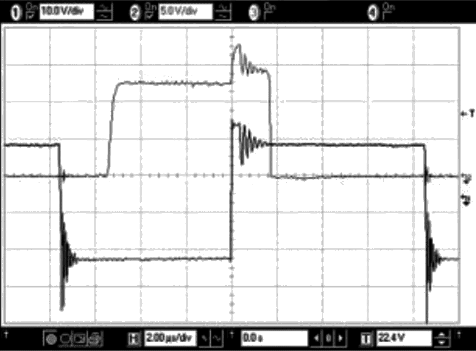
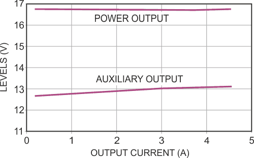
After a short period (adjustable via R1 or C1), Q2 closes and brings Q1’s base closer to ground. VCC now increases and catches up to the level at Node 2, minus Q1’s VCE(SAT). If you correctly select the time delay, VCC is devoid of any voltage spike, because you have sampled the plateau. Figure 4 shows the final result. Performing some measurements on a 70 W application board featuring low standby power yields the final tracking results in Figure 5. You can see that a 4.3 A change in IOUT results in a change of only 420 mV in VOUT. You can use the circuit in a primary-regulation application in which you need a precise level without either heavily filtering the secondary winding (and thus lowering the available auxiliary energy in standby mode) or reducing the primary clamp voltage to a higher dissipative value. In the NCP1200 application, when a short circuit appears at the output, the auxiliary winding properly triggers the short-circuit protection.
 |
|
| Figure 4. | By delaying the sampling time, you obtain a clean auxiliary level that is devoid of any leakage-inductance effects. |
 |
|
| Figure 5. | Thanks to the circuit in Figure 3, the auxiliary winding better tracks the primary winding. |