Achievement represents a crucial step in the delivery of next-generation non-volatile embedded memories
A non-volatile memory technology which is denser, faster and more cost-effective than conventional flash memory technology is closer to production, due to the continued efforts of Freescale Semiconductor to optimize the properties of silicon nanocrystals. Freescale has manufactured the world's first 24-megabit (Mbit) memory array based on silicon nanocrystals, a major step toward replacing conventional floating gate-based flash memories.
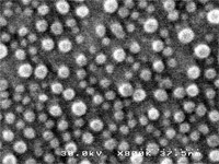
Silicon Nanocrystals
A scanning electron microscope image of silicon nanocrystals deposited using a chemical vapor deposition process. The nanocrystals serve as charge storage sites for Freescale's nanocrystal based nonvolatile memory.
The 24-Mbit memory array technology was manufactured at Freescale's Austin Technology & Manufacturing Center using 90-nanometer (nm) CMOS bulk technology. The production of a working 24-Mbit memory device requires that silicon nanocrystals be deposited with excellent uniformity and integration approaches that keep the nanocrystal properties intact during subsequent processing. In successfully achieving this, Freescale has overcome major challenges to introducing this technology into production.
As the industry begins manufacturing at smaller geometries — 90-nm and smaller — embedding floating gate-based flash becomes difficult to produce cost-effectively. At those dimensions, the chip area consumed by the 9-12V high-voltage transistors required to write and erase the conventional flash module cannot be scaled down. Furthermore, engineers cannot reduce the high voltage in floating gate-based flash without compromising reliability or risking memory failures and loss of data.
Silicon nanocrystal memories are part of an advanced class of memory technologies called thin-film storage. They are more scaleable than conventional floating gate-based flash technology, as their tunnel oxide thickness can be reduced without impacting data retention. The charge is stored on isolated nanocrystals and is lost only from those few nanocrystals that align with defects in the tunnel oxide — while the same defects would result in significant charge loss from a conventional floating gate. A thinner tunnel oxide permits lower-voltage operation, substantially reducing the memory module area needed to generate the bit-cell programming voltages, and allowing for significant wafer processing simplifications and manufacturing cost reductions. The combination of higher bit density and reduced cost translates to lower cost per bit to embed silicon nanocrystal memories. Freescale expects significant reductions in cost per bit of silicon nanocrystal thin-film storage memories.
Freescale successfully pioneered the use of nanocrystals in memory devices in March 2003, and discussed the demonstration of its first-of-its-kind 4-Mbit nanocrystal memory device at the December 2003 IEEE International Electron Devices Meeting (IEDM) in a paper entitled "A 6-V embedded 90-nm silicon nanocrystal nonvolatile memory."