By Todd Toporski, Texas Instruments
Analog Applications Journal
Enhancing immunity to RFI and other high-frequency EMI
As shown in previous sections, active filtering and CMRR can reliably reduce circuit noise in the device’s band-limited range, including DM and CM EMI up into the MHz range. However, exposure to RFI noise above the intended operating frequency range may cause non-linear behavior in the device. Op amps are most susceptible to RFI on their high-impedance differential input stage because DM and CM RFI noise can be rectified by internal diodes (formed by p-n junctions on the silicon). This rectification creates a small DC voltage or offset that is amplified and may appear as an erroneous DC offset at the output. Depending on the accuracy and sensitivity of the system, this may create undesirable circuit performance or behavior.
Fortunately, enhancing op amp immunity (or reducing susceptibility) to RFI can be achieved using one of two methods. The first and best option is to use an EMI-hardened op amp that includes internal input filtering to reject noise in the range of tens of megahertz up to gigahertz. More than 80 TI devices exist today and can be found by searching “EMI Hardened” devices on the TI op amp parametric search engine. More details on EMI-hardened op amps can be found in References 2 and 3.
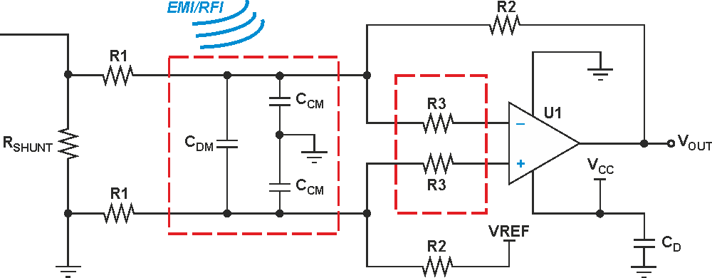
The second option is to add external EMI/RFI filters to the input of the op amp. This may be the only option if a design requires using a device that does not include internal EMI filters. Figure 2 shows a standard difference-amplifier configuration using external DM and CM filters that are targeted at higher EMI frequencies. Without input filters, the circuit gain is |R2/R1|. If passive input filters are added, R3 resistors are typically needed to prevent the CDM capacitor from reducing the phase margin of the amplifier. The DM low-pass filter consists of both R1 resistors, CDM, and both CCM capacitors. The CM low-pass filter uses both R1 resistors and both CCM capacitors.
 |
||
| Figure 2. | Passive EMI/RFI input filters improve high frequency immunity. | |
Equations for the –3-dB cutoff frequencies of the DM and CM filters (fC_DM and fC_CM) are shown below. fC_DM is set at a frequency above the desired bandwidth of the op amp circuit, and CDM is typically determined first. CCM capacitors are then chosen to be at least ten times smaller than CDM to minimize their impact on fC_DM, and because CCM capacitors are targeting higher frequencies. As a result, fC_CM will be set to a frequency higher than fC_DM. Note that an EMI-hardened device can be used to eliminate the components boxed in red and simplify the design.
 |
(3) |
 |
(4) |
Low output impedance reduces interference
Another important characteristic of op amps is their very-low output impedance, typically a few ohms or less in most configurations. To understand how this is beneficial for reducing EMI, consider how EMI impacts low- and high-impedance circuits.
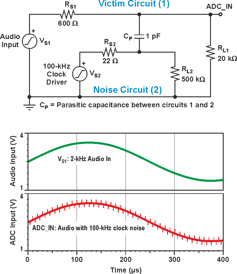
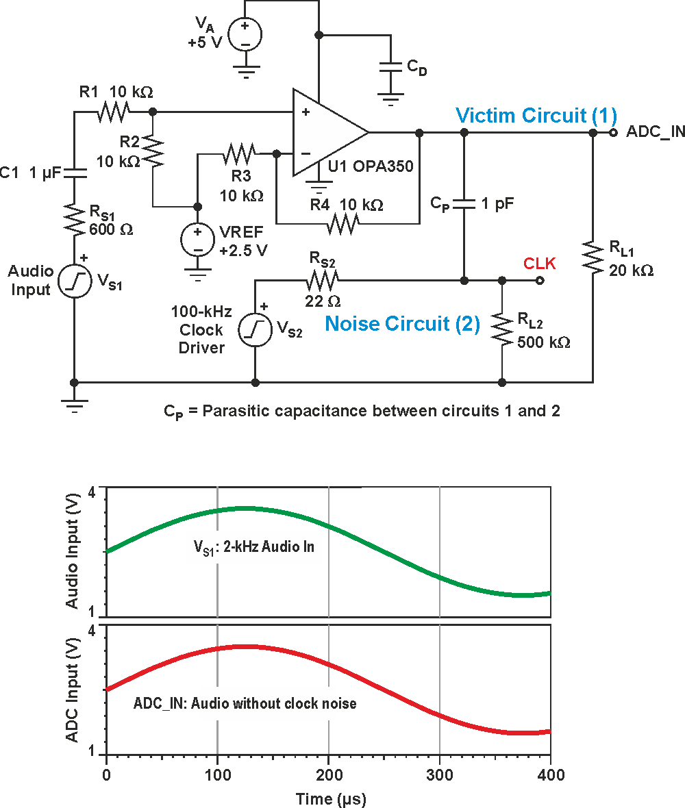
The diagram in Figure 3 represents two circuits. The first is an audio circuit that represents the input of an analog-to-digital converter (ADC) is comprised of a 1-VP-P, 2-kHz sinusoid (VS1), 600-W source impedance (RS1), and a 20-kW load impedance (RL1). Source impedances like 600 W are common in audio applications for sources such as microphones and high-input impedances like 20 kW are common for audio ADCs. The second circuit is a 100-kHz clock source driving a 3.3-V clock signal (VS2) with a series-termination resistor of 22 W (RS2) and load impedance of 500 kW (RL2). The high-impedance load represents the digital input of another device.
 |
||
| Figure 3. | Clock noise source and audio victim circuit. | |
In a real system, I2C serial bus clocks in the 100- to 400-kHz range are common around audio ADCs and circuits. Although I2C clocks are typically driven in bursts (not continuously), this simulation shows the possible impact during the time the clock is driving. A clock routed near a sensitive audio trace is a real possibility on high-density audio and infotainment PCB designs. For capacitive coupling to occur, it takes only a few picofarads of parasitic PCB capacitance to inject clock noise current into the victim audio signal. This is simulated using only 1 pF of parasitic capacitance, as shown in Figure 3.
 |
||
| Figure 4. | Op amp circuit reduces EMI from clock source. | |
How can noise be reduced in the audio circuit? As it turns out, reducing the impedance of a victim circuit is one way to reduce its susceptibility to coupled noise. For circuits with relatively high source impedance (> 50 W) coupled-noise can be reduced by minimizing the source impedance seen by the circuit load. In Figure 4, a noninverting configuration of the OPA350 is added to the circuit to buffer the signal and isolate the source impedance from the load. Compared to 600 W, the output impedance of the op amp is very low, which significantly reduces the clock noise.
Don’t forget the importance of decoupling
Adding decoupling capacitors to power supply pins is extremely beneficial in filtering high-frequency EMI noise and enhancing the immunity of the op amp circuit. All figures in this article show decoupling capacitor CD as part of the circuit. While the subject of decoupling can get complex very quickly, a few good “rules of thumb” apply to any design. In particular, select capacitors with the following characteristics:
- Very-good temperature coefficient, such as X7R, NPO, or COG
- Very-low equivalent series inductance (ESL)
- Lowest possible impedance over the desired frequency spectrum
- Capacitor values in the 1- to 100-nF range usually work well, but criteria (2) and (3) above are more critical than the capacitor value.
Placement and connections are just as critical as the selected capacitor. Place capacitor as close to the supply pins as possible. Connections to PCB supply/ground should be as short as possible with short traces or via connections.
Conclusion
Op amps can help to reduce near-field EMI on a PCB and enhance the system design. Here are some key points to consider for any design:
- Reduce input DM noise from cables/circuits using a well-chosen active filter configuration (Figure 1).
- Reduce input CM noise from cables/circuits by selecting an op amp with high CMRR and using precision matched resistors (Figure 1, Equations 1, 2).
- Further enhance immunity to high-frequency EMI or RFI (both DM/CM noise) by selecting an EMI-hardened device, or by using external passive EMI/RFI filters (Figure 2).
- Use the low impedance of the op amp output to reduce coupled noise when driving the signal to other circuits on the PCB.
- Finally, reduce supply noise by using a proper decoupling strategy for the op amp and all other circuits.
References
- S. Franco, “Circuits with Resistive Feedback,” Design with Operation Amplifiers and Analog Integrated Circuits, 3rd ed. New York: McGraw-Hill, 2002, Ch. 2, pp 75-76
- Chris Hall and Thomas Kuehl, “EMI Rejection Ratio of Operational Amplifiers,” Texas Instruments Application Note (SBOA128), August 2011
- “A Specification for EMI Hardened Operational Amplifiers,” Texas Instruments Application Note (SNOA497B), April 2013
- Jerry Freeman, “Techniques to enhance op amp signal integrity in low-level sensor applications, Part 4,” EETimes, Dec. 18, 2008