Justin Larson,Frank Kolanko
EDN
Buck regulators operating in CCM (continuous-conduction mode) have straightforward operation, allowing for easy calculation of output voltage and system design. However, lightly loaded buck regulators operate in DCM (discontinuous-conduction mode), and their operation is more complicated. The duty cycle changes from a ratio of the output voltage and the input voltage. A regulator that reduces a 12 V input to 6 V has a 50% duty cycle. When the regulator is too lightly loaded to keep some current continuously flowing in the inductor, it enters DCM. The duty cycle changes to a complex function of inductor value, input voltage, switching frequency, and output current, greatly slowing the control-loop response.
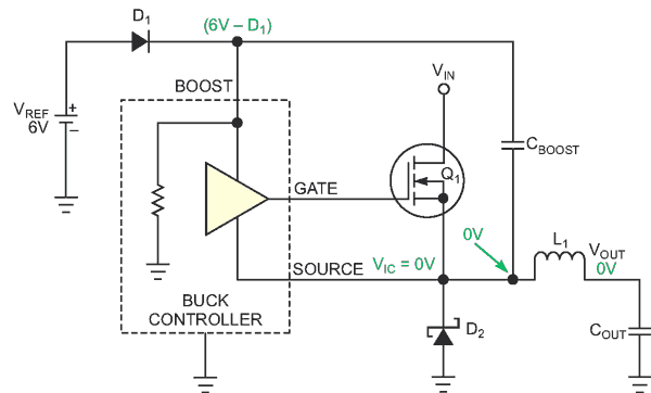
Many buck-controller ICs use a floating- gate driver (Figure 1). You use a separate supply reference voltage, VREF, for high efficiency. During start-up, it powers the NFET gate driver to a diode drop below the reference voltage. Sufficient voltage is available to drive the gate of the FET because the initial conditions dictate 0 V on the output and on the source of FET Q1.
 |
||
| Figure 1. | Many buck-controller ICs use a floating-gate driver. | |
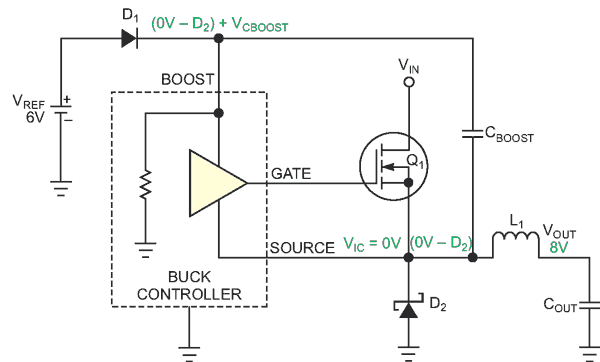
During CCM, current always flows through the inductor. Q1 or D2 supplies this current during the flyback event that Q1’s turn-off causes (Figure 2). The flyback event creates a voltage at the source of Q1, and the drop across D2 limits this voltage, making it a negative voltage with respect to ground. Sufficient voltage is available to drive Q1 because the CBOOST capacitor boosts the gate voltage. This boost provides a high voltage to the boost pin and the resultant negative voltage on the Q1 source.
 |
||
| Figure 2. | During CCM, current always flows through the inductor. Q1 or D2 supplies this current during the flyback event that Q1’s turn-off causes. |
|
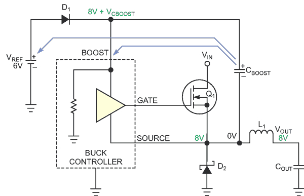
The system enters DCM when the load drops to the point at which the average current demand is less than one-half the current ripple. Diode D2 prevents reverse current in the inductor. Depending on the chip you use, the output may overshoot due to the slower response time of the control loop. The regulator may also miss pulses and generally operate unpredictably. After Q1 turns off, CBOOST starts to bleed down through the boost pin and D1 (Figure 3). The extended off time of Q1 in DCM starts to discharge the CBOOST capacitor. At approximately 3 V across CBOOST, Q1 does not turn on until the output capacitor, COUT, discharges adequately to provide a lower voltage on the source of Q1 than that of the boost pin through D1. This behavior is unacceptable in a voltage regulator.
 |
||
| Figure 3. | The CBOOST capacitor discharges when the regulator goes into DCM. | |
High temperatures create a situation with higher leakage currents. You don’t know the temperature coefficient of the current into the boost pin, so you should also check operation at low temperature. Evaluate the system to determine the lowest capacitor value, using this result in your worst-case evaluation simulations. You can thus ensure that the design will operate in DCM by increasing the value of CBOOST. You could also increase the reference voltage to which D1 connects. You may want to consider replacing D1 with a low-leakage Schottky diode. If none of these approaches results in reliable operation, you can switch to an IC that uses a gate driver referenced to ground or modify your design to use a synchronous-buck architecture.