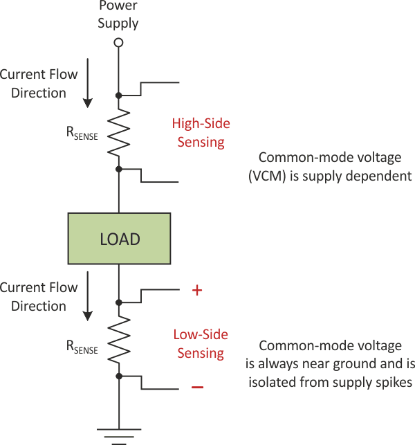
For most applications, current measurements are made by sensing the voltage drop across a resistor. There are two locations in a circuit that resistors are commonly placed for current measurements. The first location is between the power supply and load. This measurement method is referred to as high-side sensing. The second location a sense resistor is commonly placed is between the load and ground. This method for sensing the current is referred to as low-side current sensing. Figure 1 shows the two methods to sense current in a load.
 |
|
| Figure 1. | Current Sensing Methods. |
There are advantages and disadvantages of doing either measurement. One of the advantages of lowside current measurements is the common-mode voltage, or the average voltage at the measurement inputs is near zero. This makes it easier to design application circuits or select devices for this measurement. Since the voltages seen by the current sensing circuit are near the ground, this is the preferred method of measuring currents when dealing with very high voltages, or in applications where the supply voltage may be prone to spikes or surges. The immunity to high voltage spikes and ability to monitor currents in high-voltage systems make low-side current sensing popular in many automotive, industrial, and telecommunication applications. The major disadvantage of low-side current sensing is that the voltage drop across the sense resistor appears as a difference between the supply ground and the load/ system ground. This can be an issue if other circuits are referenced to the supply ground. To minimize this issue, reference all circuits that have interactions to the same ground. Reducing the value of the current sense resistor helps minimize any ground shifts.
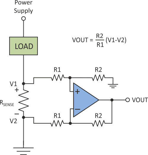
Low-side current sensing is the easiest method to use when designing circuits or choosing devices to do current measurements. Due to the low common mode voltage at the inputs, a difference amplifier typology can be used. Figure 2 shows the classical difference amplifier typology using an operational amplifier (op-amp).
When using an op-amp for current sense measurements, there are several performance requirements that need to be met to ensure correct operation. First, the operation amplifier needs to support common-mode input voltages to ground when operated from a signal supply. Since the difference amplifier typically gains the differential input signal, the swing to rail specification of the op-amp is important in order to ensure the signal is correctly passed to the output. For these reasons, rail-to-rail input and output operation amplifiers are generally preferred for current sense measurements. Since operational amplifiers are not specified in the difference amplifier configuration, it is difficult to tell what the performance can be in the real application. Parameters such as slew rate, bandwidth, input current, common mode rejection, and drift are all degraded when resistors around the op-amp are added to create the current sense circuit. The parametric degradation depends on the closed loop gain of the amplifier and values of the gain setting resistors. Figure 2 shows the matching and tolerance of R1 and R2. They need to be considered when implementing a discrete solution since variations in these components directly affect the circuit gain error.
 |
|
| Figure 2. | Operational Amplifier Configuration for Low-Side Sensing. |
Another factor to consider when implementing a discrete current sense amplifier is the PCB layout. R1 and R2 need placed as closely as possible to the operational amplifier and current sense resistor. By placing these components close the op-amp the likelihood of noise pickup on the operational amplifier positive input is reduced. Since many current sense amplifiers are used with DC/DC convertors, the placement of the entire current sense circuit needs to be carefully considered to avoid radiated noise by the DC/DC power supplies. Figure 2 shows how to calculate the difference amplifier gain. However, any increase or decrease in the gain affects the solution stability and bandwidth. The stability of the op-amp requires special consideration in applications where a capacitive load is present to avoid oscillations or excessive output ringing.
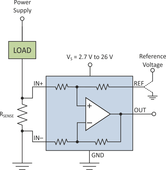
Figure 3 shows a current sense amplifier, which is an effective way to address the weaknesses of the discrete implementation.
 |
|
| Figure 3. | Low-Side Current Sensing with INA199 Current Sense Amplifier. |
A current sense amplifier integrates the gain setting resistors, reducing many of the layout concerns that exist with discrete implementations. The internal resistors are designed to reduce mismatch, which optimizes the gain error specification. Current sense amplifiers come preconfigured to address many different gain requirements. For example, the INA199 is available with gains of 50, 100, and 200 V/V. The bandwidth and capacitor load stability is optimized for each gain setting with maximum capacitive loads specified in the datasheet. Integration of the gain setting resistors reduces noise susceptibility, PCB area, and simplifies the layout. Integration of these resistors does not necessarily mean an increase in package size. The INA199 is available both in the 2- mm × 1.25-mm SC70-6 leaded package and the 1.8- mm × 1.4-mm UQFN package.
The current measurement accuracy of the INA199 is better than what is achievable with cost effective discrete op-amp designs. The device features a maximum gain error of 1.5% over the temperature range of –40 °C to 105 °C. The offset of the INA199 is less than 150 μV and drifts less than 0.5 μV/°C.
The INA199 also features a REF pin. The voltage applied at the REF pin adds to the voltage seen at the output. This is useful if down-stream devices need to have the current signal level-shifted.
Alternate Device Recommendations
For a smaller current sense solution with improved accuracy, the INA185 provides 0.2% gain error in the very small SOT-563 package. For applications requiring higher performance, the INA210-215 series of devices provide low offset (35 μV maximum) and gain error (1% Max). If a high accuracy current monitor with a digital interface is needed, the INA226 features a maximum offset of 10 μV and a gain error of 0.1%. If a small digital based current monitor is needed, the INA231 is offered in a tiny 1.68-mm × 1.43-mm package and is well-suited for portable or other space constrained applications. If a voltage output current monitor is needed with pin strappable gain settings, use the INA225.