Introduction
The high dv/dt and di/dt switching transients during MOSFET commutation are the chief sources of both conducted and radiated EMI from switching DC/DC regulators. While the optimization of PCB layout for gallium-nitride (GaN) switching devices has received recent attention, the layout of silicon power MOSFETs also requires careful consideration, given their widespread use in applications such as automotive and communications equipment systems where EMI performance is critical.
This TechNote explores EMI abatement in high-current DC/DC regulator circuits that employ a controller paired with discrete high-side and low-side silicon power MOSFETs. Using a single-sided PCB layout that specifically minimizes the parasitic inductance of the switching power loop, the switch-node voltage overshoot and ringing during MOSFET commutation are reduced, thus lowering regulator EMI signature.
Conventional Layout Designs
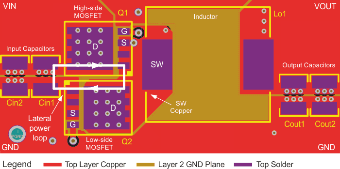
Figure 1 shows a single-sided layout of a synchronous buck regulator with discrete power MOSFETs, Q1 and Q2, in popular SON 5 × 6-mm case size. Placement of input capacitor Cin1 near the MOSFETs results in a high-frequency switching loop with lateral orientation and a relatively high area of almost 20 mm2. A layer-2 (L2) ground (GND) plane acts as an image plane for currents on the top layer, providing a flux cancellation effect. Still, the parasitic loop inductance is quite high, greater than 1 nH.
 |
|
| Figure 1. | Synchronous Buck DC/DC Regulator PCB Layout With Laterally Oriented Switching Loop. |
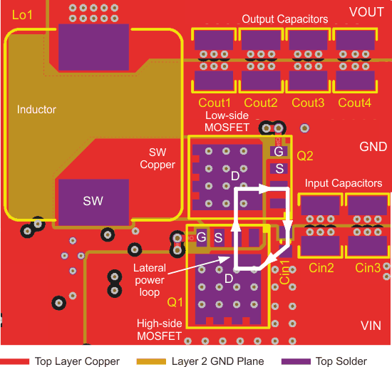
The layout in Figure 2 is modified so that the high-side FET (Q1) is rotated 90°. This improves heatsinking of Q1 for better thermal management, and allows convenient placement of capacitor (Cin1) in 0603 case size near the MOSFETs for high-frequency decoupling. Also note the U-shaped layout orientation of the power-stage components positions the output capacitors for a shorter return connection to the lowside MOSFET and input capacitors.
 |
|
| Figure 2. | Improved Lateral Switching Loop Design. |
Switching Loop Optimization
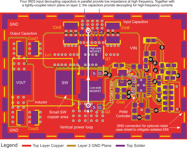
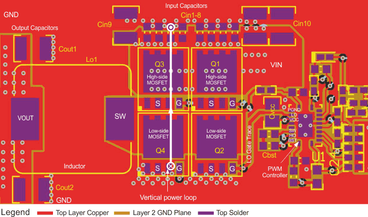
Figure 3 shows a proposed layout with the benefit of a reduced switching power loop area and lower EMI using a multilayer PCB structure. The design uses layer 2 of the PCB as a power-loop return path directly underneath the top layer to create a small physical loop area of 2 mm2. The currents flowing in opposing directions in the vertical loop configuration provide field self-cancellation, further reducing parasitic inductance.
For completeness, Figure 3 also includes the layout of the LM5146-Q1 100-V synchronous buck controller. Surround the regulator in the GND pad geometry to connect an EMI shield if needed.
 |
|
| Figure 3. | Vertically Oriented Switching Loop Design. |
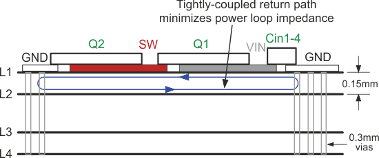
Figure 4 shows a side view to illustrate the concept of creating a low profile, self-canceling loop in a multilayer PCB structure. The L2 GND plane layer provides a tightly coupled current return path directly under the MOSFETs to the source terminals of Q2.
 |
|
| Figure 4. | PCB Stack-Up Depicting Switching Loop With Low Area Using Layers L1 and L2. |
Four 10-nF input capacitors with small 0402 or 0603 case size, designated Cin1 to Cin4 in Figure 3, are placed in parallel very close to the drain of Q1. The low equivalent series inductance (ESL) and high selfresonant frequency (SRF) of the small footprint capacitors yield excellent high-frequency performance. The negative terminals of these capacitors are connected to the L2 GND plane with multiple 12-mil (0.3-mm) diameter vias, minimizing inductance.
In addition, the switch-node copper polygon in Figure 3 includes just the pad of the inductor and the minimum area required to connect to the MOSFETs. Ground plane copper shields the polygon pour connecting the MOSFETs to the inductor terminal. The single-layer routing of traces for SW and BST means that vias with high dv/dt do not appear on the bottom side of the PCB. This avoids e-field coupling to the reference ground plane during the EMI test.
Finally, using two ceramic output caps on each side of the inductor, Cout1 and Cout2, optimizes the output current loops. Having two parallel return paths from the output splits the return current in two, helping mitigate “ground bounce” effect.
Results and Discussion
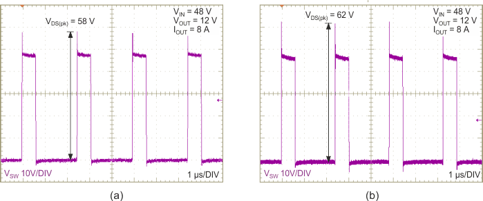
Figure 5(a) shows the switch-node voltage waveform measured with a wide-bandwidth probe using the optimized layout of Figure 3. With a parasitic loop inductance less than 500 pH, ringing is not evident, just a low-amplitude overshoot and negligible undershoot, which bodes well for EMI performance above 30 MHz.
 |
|
| Figure 5. | Switch-Node Voltage Waveforms With Vertical Loop Layout (a); Lateral Loop Layout (b). |
For comparison, Figure 5(b) shows a similar measurement using the same circuit, but with the lateral loop layout of Figure 2. The peak overshoot of the optimized layout is lower by approximately 4 V.
Extension to High-Current Applications
Figure 6 shows a layout that supports paralleled FETs. Similar to the layout technique shown in Figure 3, the four power MOSFETs, two each for high-side and low-side positions, provide additional current capability and improved thermal performance.
 |
|
| Figure 6. | Paralleled MOSFET Layout Design. |
Again, the 0603-sized input capacitors conduct high-frequency currents, while the adjacent 1210 capacitors provide low-frequency bulk decoupling.