Since its invention over a half-century ago by Hanz Camenzind at Signetics, the familiar 555 analog timer (in league with its updated pin-compatible CMOS descendants) has become an iconic design element incorporated into useful standardized functional blocks almost too numerous to count. The list includes astables, bistables, monostables, voltage converters, square waves, triangle waves, saw teeth, V-to-Fs, even PWM amplifiers.
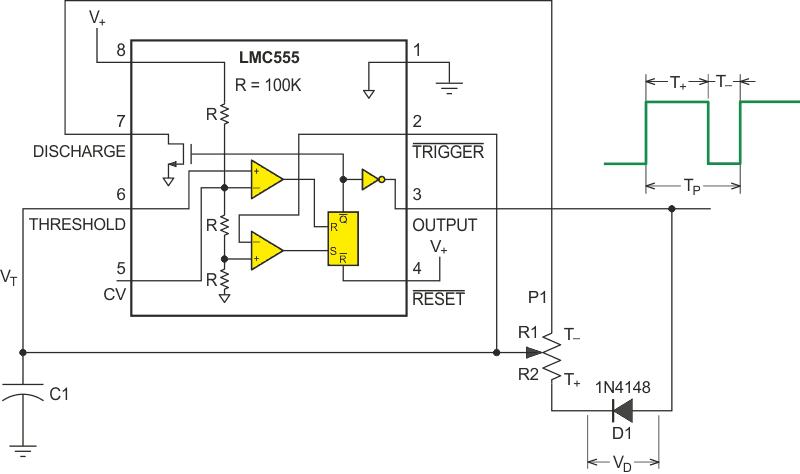
Figure 1 illustrates one of these classics: Constant-frequency oscillator with duty cycle continuously variable from 0% to 100% via single pot P1.
 |
|
| Figure 1. | Diode D1 causes temperature dependence in this 555 timer circuit. |
It works because the open-drain DISCHARGE pin of the 555 ramps C1 down through R1 (the top half of pot P1) during the T– half of the output cycle, and diode D1 steers C1 ramp up current from the 555 OUTPUT pin through R2 (the bottom half of pot P1) during the T+ positive output half-cycle, resulting in:


Unfortunately, the latter two equations differ from the usual elegant 555 V+ and temperature independent timing math because of the effects of diode forward voltage drop, VD = ~700 mV – 2 mV/°C for a typical silicon planar junction diode like the 1N4148. Consequently, the timed intervals change in response to variations in both temperature and V+ power supply. The magnitude of the changes vary inversely with nominal V+ (Table 1) and might be acceptable for some non-critical applications, but likely not when precision matters.
| Table 1. | Figure 1 error coefficients | |||||||||||||||
|
||||||||||||||||
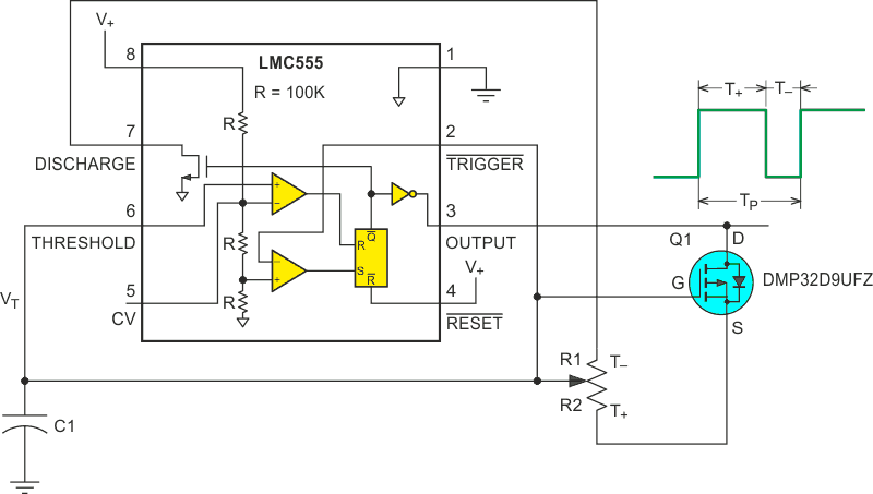
Figure 2 shows a fix: An inverted polarity p-channel MOSFET Q1 to steer C1 charging current without any significant voltage drop and thus implement new temperature and V+ independent timing design equations:


Now the variable-duty-cycle/constant-frequency function is achieved without compromising the inherent accuracy of the 555.
 |
|
| Figure 2. | An inverted polarity MOSFET Q1 restores timer precision. |
The reason Q1 is connected “inverted” with its drain pin instead of source pin connected to the positive voltage source (opposite to usual practice for a p-channel FET) is to avoid forward-biasing the FET body diode when the 555 OUTPUT pin drives the drain pin low while C1 holds the R2-connected pin high. An added benefit is, because the body diode is forward-biased when OUTPUT goes high, we’re guaranteed the FET source pin will be driven positive relative to the gate pin and the FET will go into solid saturation during the T+ interval.
| Table 2. | Figure 1 error coefficients with Schottky diode |
|||||||||||||||
|
||||||||||||||||
An interesting aside is that a version of the Figure 1 circuit is described on page 429 of the third edition of Horowitz and Hill “The Art of Electronics.” “The Art…” shows a Schottky diode instead of a junction type for D1 due to the former’s lower VD. This is a good idea as the V+ error term is significantly improved, but because the temperature coefficient of Schottkys (–2 mV/°C) is similar to that of junction diodes, temperature dependent error remains mostly unchanged (Table 2).