Sometimes, the need arises for a low-distortion buffer amplifier capable of handling bipolar signals. You can use an op amp or integrated buffer for these applications, but for more flexibility, a discrete design may prove useful. Applications include buffering the input of an ADC or the output of a DAC, or an audio line driver.
 |
|
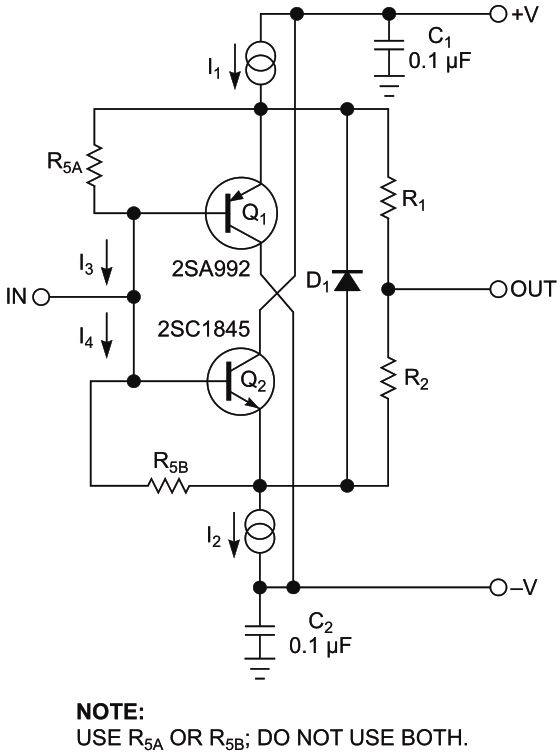
| Figure 1. | The buffer provides unity gain, low output impedance, and low distortion; see Figure 2 for details of the current sources in the transistors’ emitters. |
The buffer in Figure 1 provides unity gain, low output impedance, and low distortion. It uses two emitter followers configured as symmetrical class-A amplifiers; current sources replace the usual emitter resistors (Figure 2). To obtain the best results, you should use complementary transistors (Q1 and Q2) with closely matched dc gain (beta).
 |
|
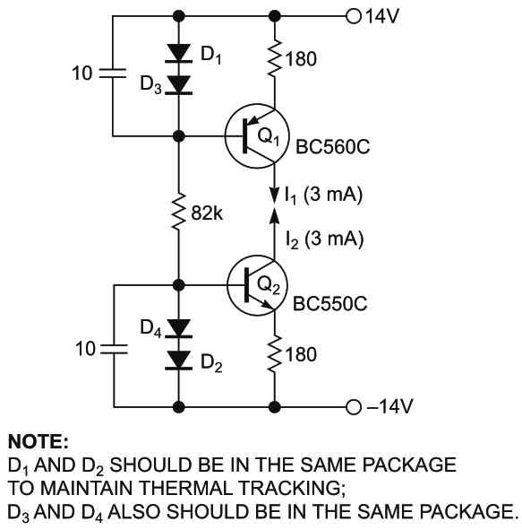
| Figure 2. | Shown are details of the current sources used in the emitters of the transistors in Figure 1. |
This topology has advantages over a conventional emitter follower. It produces a lower level of even-order harmonics and lower noise, it can provide low IBIAS and VBIAS at the input and low offset voltage at the output, and it exhibits a high power-supply rejection ratio. The circuit doesn’t require temperature compensation and is dc stable. Like conventional voltage followers, it has local feedback only. This setup is advantageous in some applications where a long feedback loop can introduce additional distortions or instability.
Resistors R1 and R2 sum the two outputs. For even harmonics cancellation, their values should be matched. Preferred devices – metal film/foil, for example – should be stable and linear, and should produce low noise.
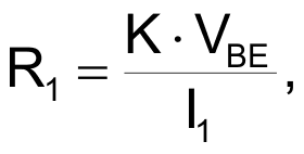
The voltage drop across R1 is equal to the base-emitter voltage, VBE, of Q1; thus,
where K is in the range of 3 to 20.
R2 is set equal to R1. The same resistors also provide stability when driving a capacitive load, so the value of K depends on this capacitance. For the ac-equivalent circuit, these resistors appear to be connected in parallel, thus providing low output impedance. Diode D1 protects the emitter junctions of both transistors from excess input voltages. When the buffer is used as an output stage, you can eliminate D1.
The dc gains of the two transistors usually are not perfectly matched, resulting in a slight output offset voltage. To compensate, note the addition of base-emitter resistors R5A and R5B in Figure 1. To reduce the output offset voltage to almost zero, you can add R5A or R5B, not both. As an example, assume that β2 > β1; R5B is then used at Q2. If Q1 has the higher beta, R5A would be used at Q1. You can estimate R5’s value from the following equation:
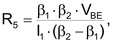
where β1 and β2 refer to the beta of Q1 and Q2.
When the output is balanced with the help of R5, input bias current is also minimized because the currents I3 and I4 cancel out each other.
 |
|
| Figure 3. | This circuit is a version of the circuit shown in Figure 1 that will automatically servo the output to a voltage close to zero. |
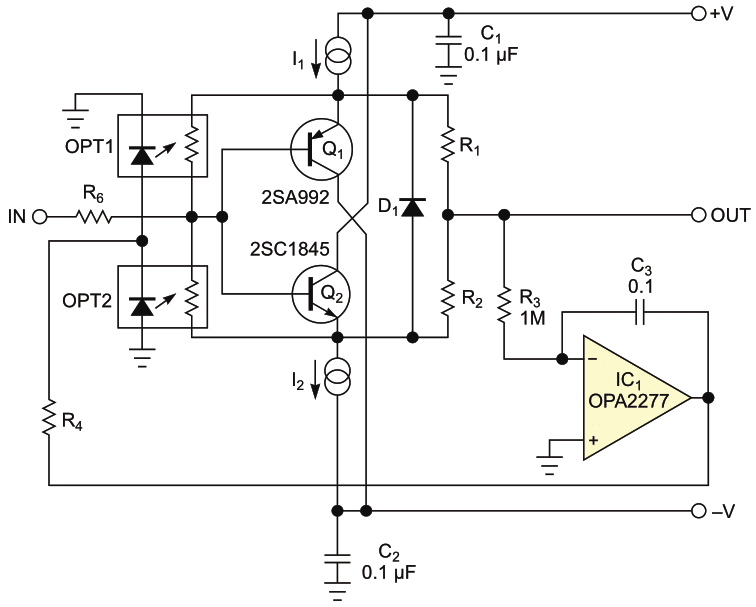
The circuit shown in Figure 3 is a version of the circuit shown in Figure 1 that will automatically servo the output to a voltage close to zero. The integrator, IC1, averages the output voltage but does not pass the ac signal, because it is acting like a high-pass filter; its corner frequency, fC, can be calculated from this equation:
In this circuit, fC is approximately 1.6 Hz.
The output of the integrator drives an optocoupler that uses a photoresistive element on the output side. This resistor replaces the upper and lower R5 resistors. The circuit in Figure 3 provides an output offset voltage of almost zero even with an input offset voltage applied, as long as it isn’t too high. The op amp, IC1, should have low noise, low bias current, and low offset voltage; also, resistor R3 and capacitor C3 should be high-quality, stable devices.
 |
|
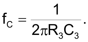
| Figure 4. | If you know which beta value is higher, you can replace one device with a diode, D2. |
One of the optocouplers in Figure 3 will always be inactive, but unless you know in advance which of the two beta values is higher, you won’t know which optocoupler is not active. High-quality photoresistor optocouplers can be rather expensive, so if you know the transistors’ beta values, you can replace one device with a diode, D2, as shown in Figure 4. In this version, β2 > β1, so the photoresistor shunts Q2. R4 also can be omitted if the optocouplers’ LEDs can tolerate the maximum output current from the integrator.
 |
|
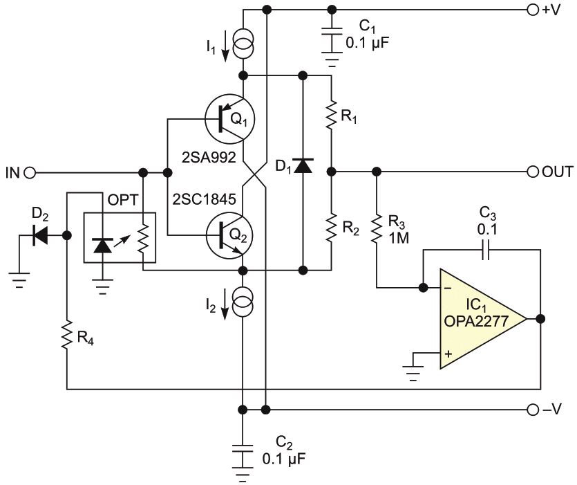
| Figure 5. | An optocoupler with an incandescent lamp can be used; in this case, the integrator is not needed, because the filament acts as an integrator. |
Incidentally, an optocoupler with an incandescent (filament type) lamp can be used; in this case, the integrator is not needed, because the filament acts as an integrator. Change the integration capacitor to 1M and the input resistor value to 1k (Figure 5). The last circuit has low dc gain (compared with the integrator), so the output dc offset can be rather high – tens of millivolts. Diode D2 prevents possible “latching” of the circuit.