Digital gates are fundamentally analog in nature. They use transistors. Sure, these transistors are operated at their conduction extremes (which is why they are called “digital”), but during the logic state transition they're pure analog. By adding a few passive components, you can make circuits such as level converters, frequency multipliers, phase detectors, line drivers, and pulse changers.
Take the simplest form of a passive component attached to a gate. A pull-up/pull-down resistor sets the logic level to an unused digital input (an absolute must with discrete CMOS). Open drain/collector/emitter outputs also require a pull-up/pull-down resistor to set the digital levels using analog means.
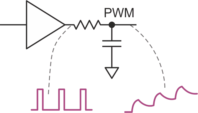
But it gets more interesting when we look at how we can use gates along with passives as timing or averaging elements. The most basic duty-cycle to analog-level conversion is accomplished with a simple RC filter in Figure 1.
 |
|
| Figure 1. | Adding an RC filter to a logic gate produces a level voltage output with ripple. |
Pulse-width-modulation (PWM) derives an analog DC voltage level that results from the timing ratio between the successive high and low logic levels applied to the RC filter network. Starting from 0 V on the capacitor, each successive high pumps the capacitor a little higher in voltage until an equilibrium is reached after about five RC time constants. There will always be a small ripple on the averaged DC level (exaggerated in the figure). For best results, make the pulse frequency as high as possible, and make the RC time constant as long as possible – consistent with the required settling time.
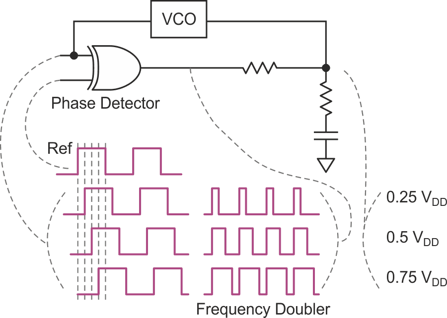
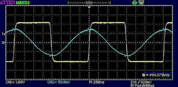
We can take advantage of this effect in the most basic of digital-type phase detectors (Figure 2). The exclusive-OR function can be used in phase-locked-loops because the RC-filtered output voltage is directly proportional to the duty cycle resulting from the phase difference between its two input signals.
 |
|
| Figure 2. | An XOR gate, voltage-controlled oscillator, and a few passive components make a frequency doubler. |
Feeding this RC filtered DC level back to the VCO servos its frequency into lock with the reference frequency. The resulting phase difference between the VCO output and the reference depends on the voltage that the VCO requires to run at the same frequency as the reference.
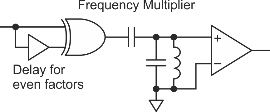
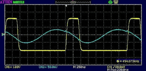
A side-effect is the frequency doubling aspect of the XOR phase detector. In fact, a similar effect can be harnessed as a frequency multiplier (Figure 3).
 |
|
| Figure 3. | Make a frequency multiplier with a XOR gate, an op amp, two capacitors, an inductor, and a delay. |
The logic edges at the XOR output ring the LC tank, which is tuned to resonate at the desired harmonic frequency. Odd harmonics are available when the XOR output is a symmetrical 50 percent duty cycle, even harmonics can be picked off with a delay line that sets the XOR output pulse duty cycle to maximize the desired harmonic. The amplifier restores the LC tank ringing to digital logic levels.
Phase detectors, line drivers, and pulse shapers
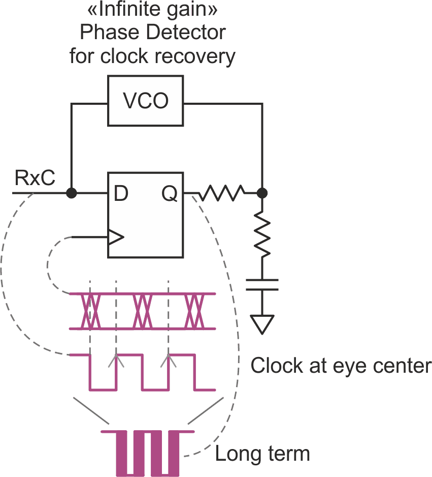
There are instances when we really want the phase relationship between the reference and the VCO (voltage-controlled oscillator) to be tightly controlled. In this situation, the XOR phase detector shown in Figure 2 doesn't quite cut it. An example is when the reference is a random NRZ (non-return-to-zero) data stream, and we want to phase-lock a VCO to generate a recovered clock such that the rising clock edges occur at the very center of the data eye pattern seen on an oscilloscope.
Since the data transitions of a weak signal get “jittery” in time due to thermal noise (among other causes) in the receiver, the best time to sample the data as to being a one or a zero is at the time farthest away from the transitions – i.e., the eye center at the amplitude peaks of the analog modulation waveform.
Here, the incoming data stream clocks the D-type flip-flop, sampling at that instant whether the VCO clock is high or low. (Only the rising data edges do the clocking; an XOR with a delayed input could allow clocking on both rising/falling data edges but not necessary.) The averaged DC output feeds back to the VCO to servo it to where the VCO falling clock edge seeks out the data transitions. Thus, the rising clock edge that actually samples the data bit is in the eye center where it belongs. This requires a 50 percent duty clock, which can easily be obtained by using a VCO at twice the desired frequency and dividing by two.
Where long runs of consecutive 1s and 0s are present in the data stream, a timed tri-state pump-up or pump-down pulse would be preferable unless the RC time constant is made very long relative to the run of consecutive bits.
This is the only use of digital logic that I know of that tolerates a D flip-flop seeking out its own point of metastability, but it doesn't matter; the occasional metastable result is but a drop in the bucket during integration of thousands of pulses by the RC filter.
Of course, the D flip-flop must be chosen for fast setup/hold times relative to the data bit rate, and there will be some drift with temperature and power supply variations through the setup/hold specs. “Infinite gain” is a bit of a misnomer; it refers to the fact that a D flip-flop, when operated in violation of setup/hold times, will either go high, low, or oscillate as a result of extremely small changes in its data/clock timing violations. Strange, but it does work.
The last time I used this technique was with a 74AHC74 D flip-flop as the phase detector. The resulting digital output looked something like the bottom waveform of the Figure 4. I might have been able to remove the back-and-forth frequency fluctuations with more attention to the RC filter parameters, but the boss was a-chomping at the bit to move on to the next crisis and the loop worked well enough for our purposes.
 |
|
| Figure 4. | A D-type flip-flop and a VCO lets you set a sampling point in the center of a signal eye diagram. |
Another use for complementary digital outputs is as a push-pull (yeah, I know, a very retro term) transformer driver (Figure 5).
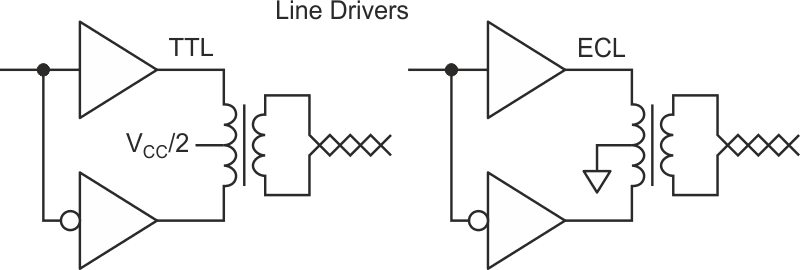 |
|
| Figure 5. | Transformers turn logic gates into live drivers. |
VCC/2 at the center tap lets the voltage induced on the logic high side (due to the pulldown on the logic low side) from becoming diode clamped to VCC with some logic families. I've used this technique with 74S series TTL with the center tap at VCC and got away with it on a prototype, but would not recommend this for a production design. Never tried this with 74(A)HC, only ECL and 74S TTL. With the stronger source drive of AHC the center tap might not be needed.
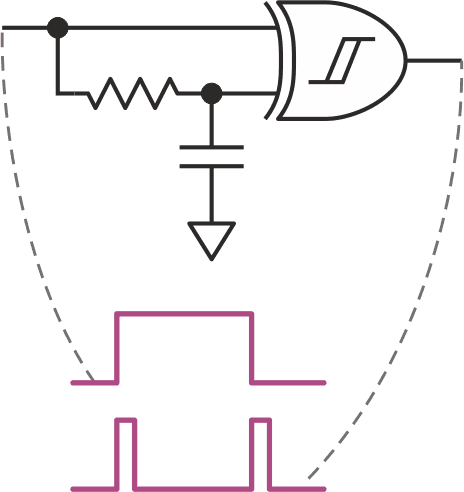
So far, all these passive components have been applied to the gate outputs. Here are some neat things that can be done at gate inputs, assuming they are Schmitt-trigger gates (Figure 6).
 |
|
| Figure 6. | Use Schmitt-trigger XOR, OR, or AND gates to make pulse shapers. |
More details on these arrangements can be seen in my EDN Design Idea (Ref. 1).
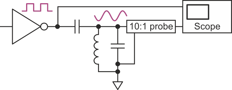
Driving a resonant LC tank circuit
Now we'll have a look at the neat things that you can do by driving a resonant LC tank circuit from a logic gate. Figure 3 touched on this. Now, let's have a peek at a bit more detail. Figure 7 shows the circuit.
 |
|
| Figure 7. | A series of logic edges at a sub-harmonic of the tank resonant frequency will cause it to ring. |
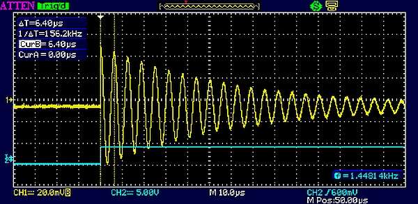
Figure 8 shows the response of a tank tuned to 156.2 kHz to a single rising edge.
 |
|
| Figure 8. | A single blue edge twangs the yellow tank like a guitar string. (Note all of the following figures have the colors swapped.) |
The tank circuit in Figure 7 uses an adjustable (ferrite slug tuned) 396 nH inductor in parallel with a 1 nF C0G (aka NP0) capacitor, and is loosely coupled to the TTL source through a 68 pF capacitor. It is not built on copperclad board or a PCB; the components are lying on the benchtop with their leads soldered together in the air. The inductor Q is spec'd on the data sheet about 88 at 40 MHz, so its Q (RF resistance/reactance) will be somewhat higher at the resonant frequency here of 8 MHz. The capacitor ratio depends on inductor Q (generally the capacitor Q is much better than the inductor Q), driver rise time, desired sine wave level, and following amplifier gain to restore the sine wave zero crossing to a digital edge.
In this case, for demonstration purposes the amplifier is represented by the oscilloscope, and the logic source is the TTL output of a function generator terminated into a 75 Ω cable and 75 Ω resistive load. Due to limitations of the function generator, the duty cycle is actually 48 percent, not the ideal 50 percent.
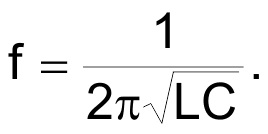
The 8 MHz resonant frequency is derived from the formula
But, the scope display in Figure 9 shows a frequency of the triggering yellow edges of 1.6 MHz – one fifth of the tank sine wave's frequency. This circuit is performing as a x5 frequency multiplier, and, in practice, odd harmonics up to the 11th or more are achievable depending on inductor Q. (I say 11th because that is the highest I've ever attempted.)
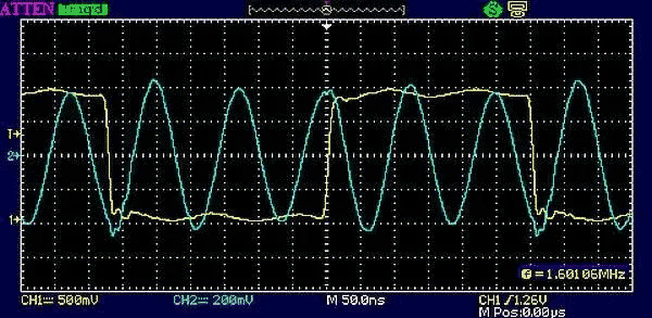 |
|
| Figure 9. | A series of yellow edges at about 50% duty cycle result in continued blue ringing if the edges are timed properly. |
There's something else about the phase relationship between the driving edges and the sine wave peaks. The rising edge correlates with the positive peak, the falling edge with the negative peak. Therefore an even harmonic cannot be picked off of a 50 percent square wave – the alternating edges would cancel the same-polarity sine peaks. (Mr. Fourier was right!)
But with a slight shift in the edge duty cycle we can make the sine peaks line up again at an even harmonic, such as the x6 multiplier in Figure 10.
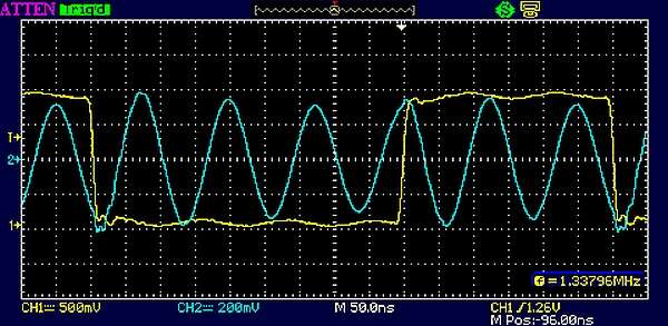 |
|
| Figure 10. | Here we have a 40% duty cycle 1.333 MHz digital signal exciting the 6th harmonic, again at 8 MHz for demo purposes because I didn't want to mess with re-tuning the tank. |
Figures 11 and 12 show how the harmonic multiplication factor changes as the duty cycle changes. The ringing frequency is still constant at 8 MHz since the tank component values have not been changed, but now the rectangular wave frequencies are at the sub-multiples of 1/7 (1.14 MHz) and 1/8 (1 MHz) of 8 MHz respectively.
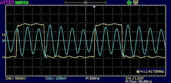 |
|
| Figure 11. | A 35% duty cycle rings the 7th harmonic of a 1.14 MHz rectangular wave. |
And so on. As long as the alternating digital edges can be made to fall on the alternating peaks of the resulting sine wave, the tank will ring. To put it another way, the timing between alternating digital edges must equal an integral number of half-periods of the desired harmonic.
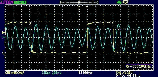 |
|
| Figure 12. | A 31% duty cycle rings the 8th harmonic of a 1 MHz rectangular wave. |
Driving pulse length
Previously we found that the duty cycle on a driving square wave affects the relationship between its rising and falling edges and the peaks of the tank circuit (Figure 7). Creating the required pulse lengths is, however, another story. This is usually not done digitally; that would require the same high-frequency clock we are trying to recreate!
Perhaps a very-high-frequency clock and counter chain could be triggered from the low-frequency edge we want to multiply and synthesize the desired pulses. But there are analog methods (as discussed earlier) using monostable multivibrators, RC networks with gates, and delay lines using readily available lumped LC with logic gates devices or actual terminated transmission line for the higher frequencies. It is even possible to get double the use out of a length of transmission line by not terminating it, and using the round-trip time of the reflected pulse as the timing element, but this can get tricky.
Now we come to an interesting case where the driving pulse is a half-cycle or less of the sine wave. Because of the limitations of the function generator I had to lower the tank resonant frequency to get the desired duty cycle. The tank circuit used to generate the waveforms in Figure 13 uses a 1 µH inductor (Q unknown, is actually a very small RF choke from the junk box) in parallel with a 100 nF capacitor, and the coupling capacitor to the digital drive had to be increased to 270 pF. The resonant frequency of the new tank is about 500 kHz. The function generator output is now the main (not TTL) output with reduced rise time since the faster TTL edges excited a parasitic ringing – possibly the self-resonance of the RF choke.
 |
|
| Figure 13. | The 50% duty cycle edges line up with every sine wave peak, and the pulse edges straddle the sine zero crossing. |
So what's the point of turning a square wave into a sine wave of the same frequency? Among other things, you can remove high frequency jitter outside of the tank bandwidth (the higher the Q, the better), especially when recovering a bit clock from a noisy serial bit stream (as in Figure 14).
 |
|
| Figure 14. | At 20% duty cycle the pulse edges still straddle the sine zero crossing. In this situation the pulse width itself is not overly critical; sloppy timing methods (within reason) to create the pulse width are acceptable. |
Figure 15 shows a square wave driving the XOR to drive the tank with a narrow pulse (as in Figure 14) at every rising and falling edge, but it could just as easily be a densely-coded serial bit stream such as biphase or Manchester where there are always either one or two edges per bit. Each edge rings the tank tuned to double the bit rate; a simple divide-by-two is all it takes to recover the serial bit clock. Even at minimum transition density of one edge per bit, the tank rings to fill in the missing edges and keep the recovered clock going. I've used this clock recovery method at 250 Mbit/s on 4b5b encoded serial data.
 |
|
| Figure 15. | An XOR Schmitt trigger easily creates the sloppy pulses of Figure 3 with a simple RC network. |
This can be much cheaper than a PLL (phase-locked loop) with a VCXO (voltage-controlled crystal oscillator), as long as you don't mind the fact that the tank initially needs to be tweaked into tune. It takes about the same effort as tuning one-sixth of a guitar.
Other uses for digital logic tanks include variable phase shifting, automatic phase correction of a serial bit stream sample clock, frequency translation, packet clock startup, and clock synthesis through frequency addition and subtraction (heterodyning) using an XOR gate as a frequency mixer.