When tasked with a current sensing requirement, designers typically look first to using dedicated resistors designed for this task. Occasionally though there is the temptation to consider sensing current in a printed circuit board (PCB) trace.
Current sensing resistors, commonly called current shunts, are required to accurately sense current in a load. These current shunt resistors are placed in series with the load and develop a voltage proportional to the current flowing through the shunt. In high current applications, these resistors can become large and dissipate considerable power in the form of heat. These conditions suggest that using an existing copper trace on a PCB might present a solution.
There are other difficulties in using the copper trace as a shunt; most notably, the resistance of copper is very low, meaning that the signal voltage will either be so small as to require relatively challenging amplification, or that the length of this resistor may add cost due to the PCB area required. This area usage is also impacted by the required resistance tolerances. While a narrow resistor pattern would decrease the length and thus also the area, PCB etch tolerances usually dictate a minimum width of 0.015 to 0.025 inches.
Another difficulty is the copper temperature coefficient of +0.39%/°C, meaning that the voltage drop for a given current will increase 20% for a 50 °C temperature rise. Also note that dimensional tolerances directly affect the resistor’s value. Edge control of the PCB etch process will usually define the minimum acceptable width.
Accurate copper trace current sensing
A method for solving the temperature coefficient problem to be discussed here takes a page from on-chip circuit design techniques that exploit geometric ratioing to establish circuit gain, rather than using absolute values. Even this method is not without difficulty since voltage drops will be exceedingly low, often below 10 mV. Luckily, modern zero-drift (auto-zero or chopper) op amps supply a ready solution to the low drop problem. As will be seen, there remain some limitations in achieving initial accuracy, although once calibrated, the method can be very accurate.
The idea here is to create two resistors with a geometric relationship that will define our gain. For example, consider a high current path (to be called RSHUNT) with the following (normalized) dimensions: length (L) = 1, width (W) = 10. For the gain setting element (to be called RG) create another pattern is L = 10, and W = 1. This gives a dimensional, and therefore resistance, ratio of 100:1. Since the gain resistor is intended to temperature compensate the high current RSHUNT path, it should be located symmetrically and in proximity to the RSHUNT element.
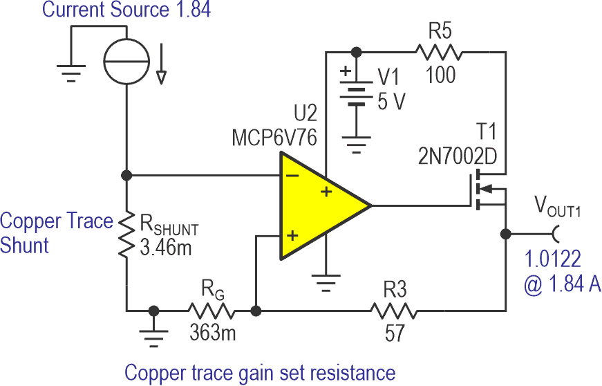
A basic circuit that was used in the initial testing of the concept as illustrated in the simplified schematic (Figure 1). The op amp drives a MOSFET that supplies the feedback current required through the gain resistor, as well as a voltage output proportional to the measured current. This is a basic circuit designed for “low-side sensing” where one terminal of the current shunt is grounded, and the amplifier output is referred to ground.
 |
|
| Figure 1. | Basic circuit is shown for low-side current sensing with temperature compensated copper PCB trace shunt. |
Note that this circuit requires an op amp with an exceedingly low input offset such as that provided by zero-drift amplifiers.
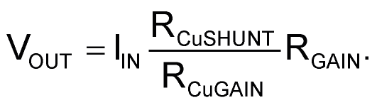
Also note in the simplified schematic that the current through R3 and RG is always a function of the input current and the ratio of the RSHUNT and RG resistors. The actual values of RSHUNT and RG are only required to have a total value such that the current flow is within the required limit of the current IT1 in MOSFET T1. The ratio of RSHUNT and RG can be determined from:
 |
|
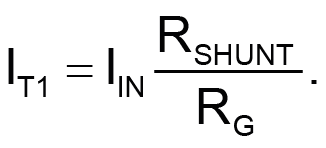
| Figure 2. | Here is how the design drawing of intended shunt and gain resistor traces looks like. |
This current sets a ratio where the output current is a fraction of the input current proportional to the geometric ratio. The voltage at the top of R3 is used as the output and can be varied to adjust gain to any desired value. An example of a circuit board layout depicting the RSHUNT and RG are shown in the low-side current sensing circuit in Figure 2 and Figure 3.
 |
|
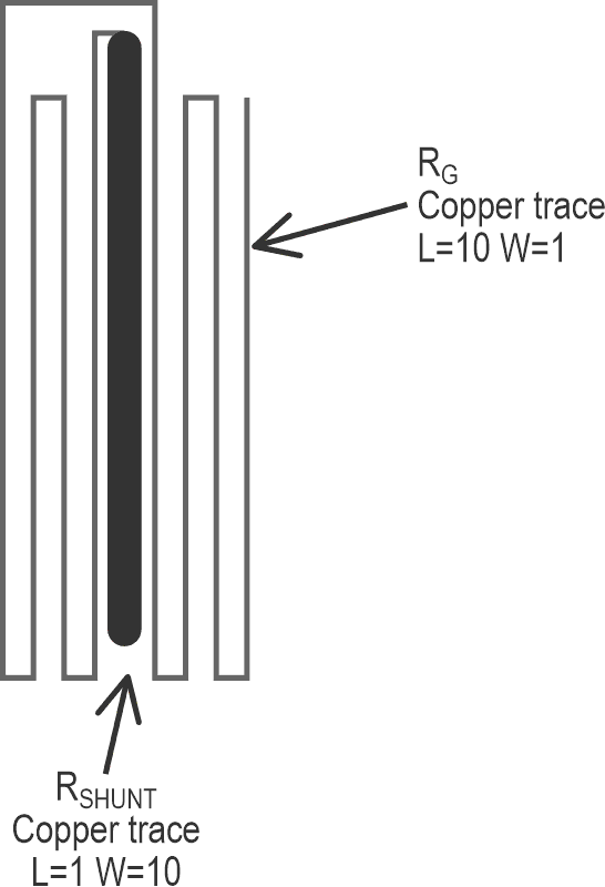
| Figure 3. | Closeup of the test board with a quarter is aimed to indicate actual size. The trace from TP6 to TP7 is the shunt RSHUNT and the trace from TP6 to TP8 is the copper gain resistor RG. The portion covered by the quarter is an unused duplication of the circuit. |
Figure 2 shows a conceptual drawing of ratio matching a copper PCB trace gain resistor to a copper PCB trace shunt to minimize initial errors as well as errors over temperature. The layout of the resistors exploits ratios and interdigitating.
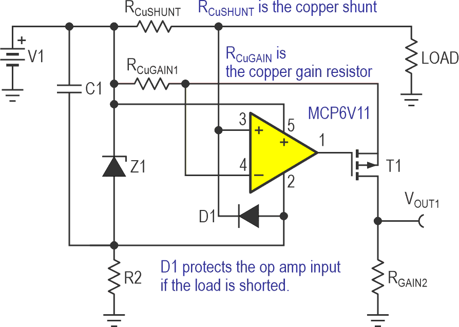
High-side current sensing implementation
A high-side sensing version can be built based on the well known “current drive current sensing” circuit shown in Figure 4.
 |
|
| Figure 4. | The current drive current sensing circuit is illustrated for high-side sensing. |
The current drive circuit is readily adapted to the trace compensation method where RCuSHUNT and RCuGAIN1 are the PCB traces. RG is a conventional resistor to set to the overall desired gain level. Z1 is a rail-to-rail Zener voltage regulator for the op amp. D1 provides input protection in case the load is shorted.
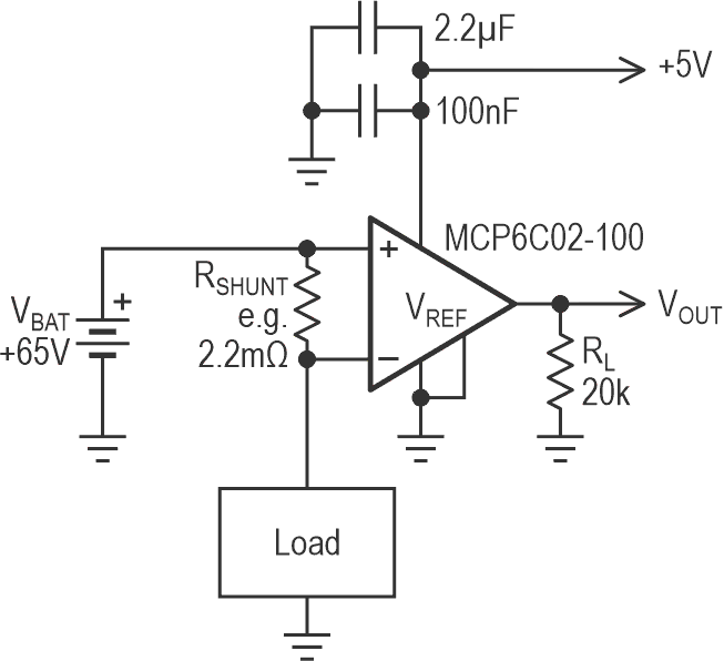
Consider dedicated shunt current sensing
When you implement current sensing on PCB traces, you soon discover why humans invented resistors. Invariably the PCB space required to implement accurate PC trace sensing will require significantly more board area than a shunt.
Keep in mind that the best amplifier offsets are on the order of 5 to 10 µV and decent accuracy begins at full scale voltage drops an order of magnitude above that. By the time you factor in all considerations, you will find that the physically smallest solution will favor the dedicated shunt resistor.
An example is shown in Figure 5 that illustrates simplicity of using dedicated shunt resistors and current sensing amplifiers. The shunt provides a precision resistance along with a low temperature coefficient. Modern zero-drift low offset current sensing amplifiers permit lower shunt voltage drops, which improves efficiency and often permits physically smaller shunts, thanks to lower shunt power dissipation. Unidirectional as well as bi-directional circuits become comparatively painless.
 |
|
| Figure 5. | Dedicated current sensing circuit uses a current sense amplifier. |