I’ve recently published Design Ideas (DIs) showing circuits for linear PWM programming of standard bucking-type regulators in applications requiring an output span that can swing below the regulator’s sense voltage (VSENSE or VS). For example: “Simple PWM interface can program regulators for VOUT < VSENSE” (Ref. 1).
Objections have been raised, however, that such circuits entail a significant loss of programming analog accuracy because they rely on adding a voltage term typically derived from an available voltage (e.g., logic rail) source. Therefore, they should be avoided.
The argument relies on the fact that such sources generally have accuracy and stability that are significantly worse (e.g., ±5%) than those of regulator internal references (e.g., ±1%).
But is this objection actually true, and if so, how serious is the problem? How much of an accuracy penalty is actually incurred? This DI addresses these questions.
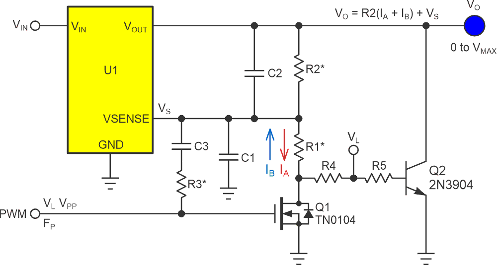
Figure 1 shows a basic topology for sub-VS regulator programming with current expressions as follows:
 |
|
| Figure 1. | Basic PWM regulator programming topology. |
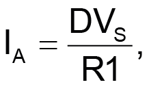
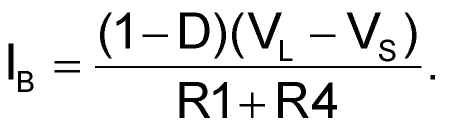
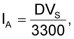
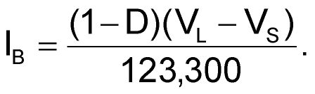
here IA is the primary programming current and IB is the sub-VS programming current giving an output voltage:

Inspection of the IA and IB current expressions shows that when the PWM duty factor (D) is set to full-scale 100% (D = 1), then IB = 0. This is due to the (1 – D) term.
Therefore, there can be no error contribution from the logic rail VL at full-scale.
At other D values, however, this happy circumstance no longer applies, and IB becomes nonzero. Thus, VL tolerance and noise degrade accuracy, at least to some extent. But, by how much?
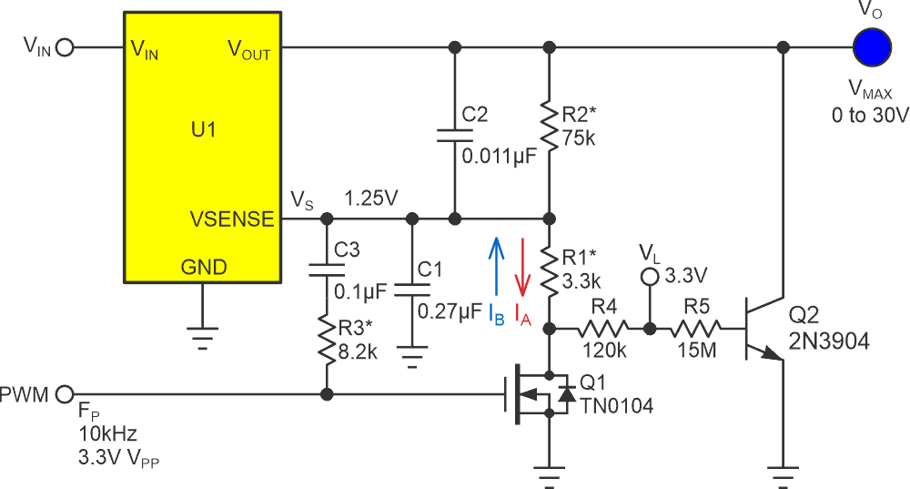
The simplest way to address this crucial question is to evaluate it as a plausible example of Figure 1’s general topology. Figure 2 provides some concrete groundwork for that by adding some example values.
 |
|
| Figure 2. | Putting some meat on Figure 1’s bare bones, adding example values to work with. |
Assuming perfect resistors, nominal R1 currents are then:

Then, making the (highly pessimistic) assumption that reference errors stack up as the sum of absolute values:
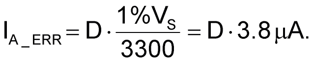
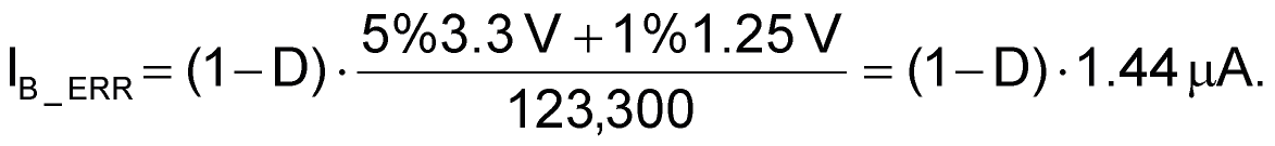
VOUT total error =

The resulting VOUT error plots are shown in Figure 3.
 |
|
| Figure 3. | VOUT error plots where the x-axis is D and y-axis is VOUT error. Black line is VOUT = VS at D = 0 and red line is VOUT = 0 at D = 0. |
Conclusion: Error does increase in the lower range of VOUT when the VOUT < VSENSE feature is incorporated, but any difference completely disappears at the top end. So, the choice turns on the utility of VOUT < VSENSE.
Reference
- Woodward, Stephen. Simple PWM interface can program regulators for Vout < Vsense