William Lepkowski
EDN
Many low-dropout voltage regulators include an enable-input pin that can also serve as an inexpensive alternative to a voltage-supervisor IC. Although the enable pin normally serves as a means of shutting down the regulator's output to save power, a few discrete components ensure that the regulator's output will turn on and off at appropriate input voltages. Thus, you can use the circuit as a voltage supervisor or as a controlled-characteristic linear-voltage regulator.
 |
||
| Figure 1. | Connecting a low-dropout regulator’s enable pin directly to the unregulated voltage input forces the output voltage to track the input voltage during the regulator’s turn-on and turn-off intervals. |
|
A typical low-dropout regulator's internal enable circuit comprises a voltage comparator that determines whether the voltage at the enable pin is either larger or smaller than an internal reference voltage, VREF. Although you can create a low-dropout voltage supervisor by directly connecting the enable pin to the unregulated input voltage, this circuit's turn-on and turn-off voltages equal the reference voltage, which typically falls below the minimum operating voltage that most ICs powered by the regulator's output require.
 |
||
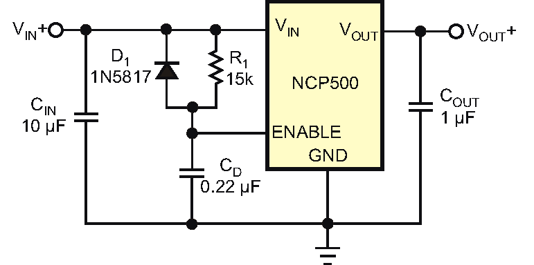
| Figure 2. | An alternative to directly connecting the regulator’s input and enable pins, this “conventional” modification uses a resistor and a capacitor to delay the regulator’s turn-on time. The diode eliminates the powerdown delay interval. |
|
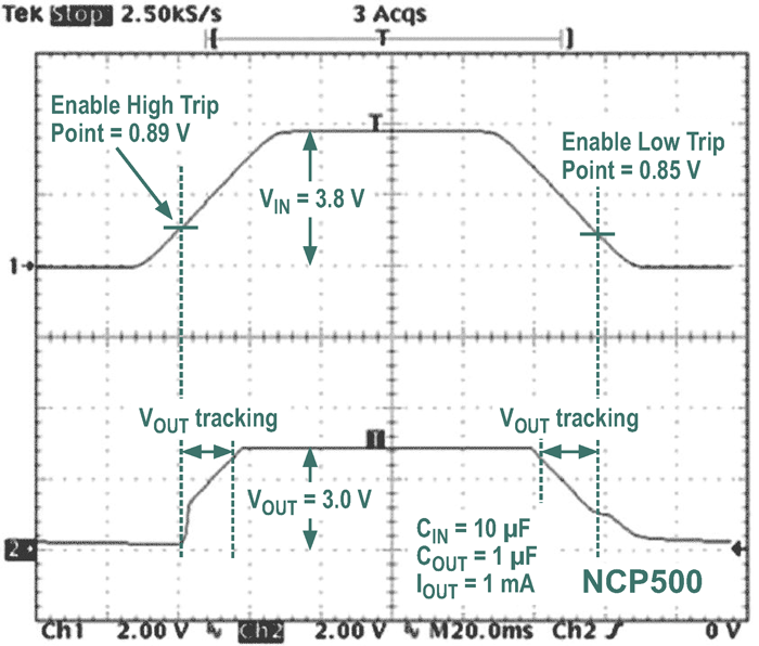
In addition, directly connecting the enable pin to the unregulated input doesn't provide a turn-on delay to ensure that the input voltage has reached a value higher than the low-dropout regulator's dropout voltage. The directly connected circuit has unsatisfactory power-up and power-down characteristics (Figure 1). As a first-order improvement, you can enhance the circuit's performance by adding R1, CIN, and D1 to provide a start-up delay for the voltage regulator's enable pin (Figure 2). Unfortunately, the external delay network improves the output's rising-edge characteristic, but its falling edge continues to track the input voltage (Figure 3).
 |
||
| Figure 3. | The added components in Figure 2 eliminate the problem of rising-edge output-voltage tracking. However, the falling-edge output voltage still tracks the input voltage. |
|
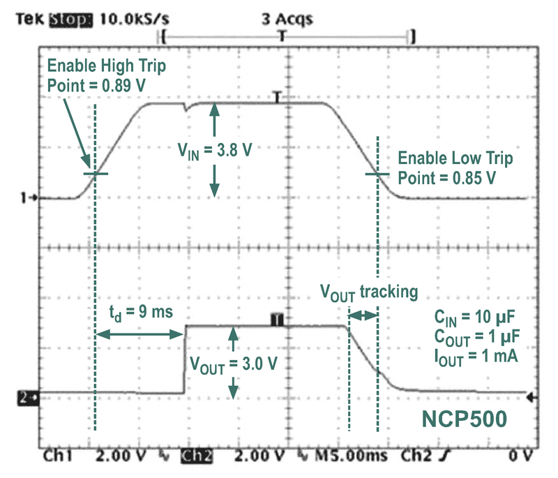
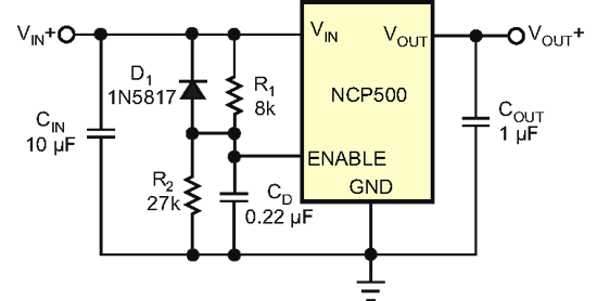
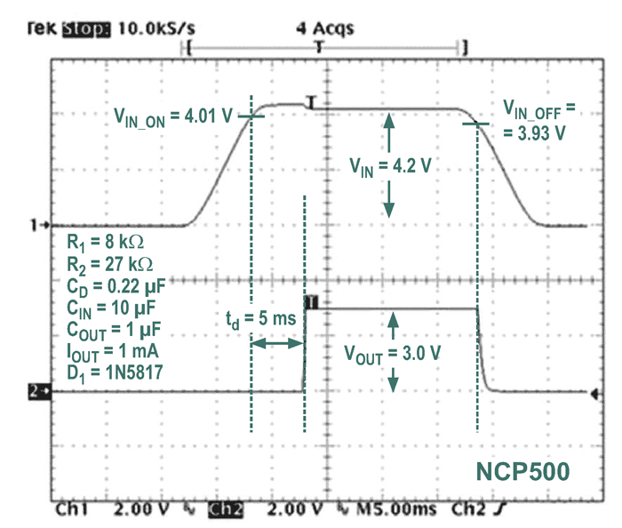
You can solve the circuit's shutdown problem by replacing the single resistor with a voltage-divider network (Figure 4). Resistor R2 raises the switching threshold of the regulator's enable pin and "tricks" the enable comparator into turning on at a higher voltage. The regulator's output then exhibits an adequate start-up delay and cleanly switches on and off (Figure 5).
 |
||
| Figure 4. | Resistor R2 increases the enable pin’s switching threshold voltage. | |
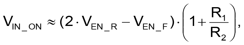
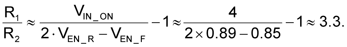
You can use Equation 1 to calculate the values of resistors R1 and R2 to alter the enable pin's threshold voltage in the circuit in Figure 4.
 |
(1) |
where VIN_ON is the user-defined turn-on voltage, VEN_R is the enable pin's rising-edge trip-point voltage, and VEN_F is the enable pin's falling-edge trip-point voltage. For example VIN_ON = 4 V, VEN_R = 0.89 V, and VEN_F = 0.85 V. To prevent the regulated output voltage from tracking the input, set the minimum value of VIN_ON to VOUT + VDRP, where VDRP is the dropout voltage.
 |
(2) |
If you select a value of 8 kΩ for R2, then R1=3.3×R2, or approximately 27 kΩ.
 |
||
| Figure 5. | The addition of R2 in Figure 3 solves the falling edge problem, and shutdown occurs immediately after the input voltage drops too low. The regulator’s output switches on only after sufficient voltage is present at its input. |
|
Equation 1 calculates only approximate values for the voltage-divider resistors, which may vary slightly depending on the voltage regulator's characteristics. If the resistors' values are too low, the regulated output tracks the input, a problem that you can easily solve by increasing the value of R1. Also, R1 and CD determine the regulator's turn-on delay time, and CD's capacitance should ideally be 0.01 to 0.47 µF. Too large a value increases the discharge time and reduces the circuit's effectiveness as a voltage supervisor.