Portable battery-powered devices often spend most of their life in standby mode, in which the quiescent current of an internal boost converter continuously bleeds the battery. The quiescent current during standby can be larger than the actual load current. Though several inductor-based converters offer maximum quiescent current of less than 10 µA, designers usually prefer or require a regulated charge pump for cost-sensitive designs that must be intrinsically safe. Off-the-shelf regulated charge pumps with output-current capabilities of at least 10 mA have typical minimum quiescent currents of 50 to 100 µA. If that level of quiescent current is unacceptable, you can reduce the overall average by adding circuitry that remotely monitors the regulated voltage and toggles the charge pump into and out of shutdown. That approach, however, may not achieve the desirable quiescent-current level of less than 10 µA. The advent of low-on-resistance analog switches and ultralow-current comparators and references makes possible a charge-pump circuit whose maximum quiescent current is approximately 7 µA (Figure 1).
 |
||
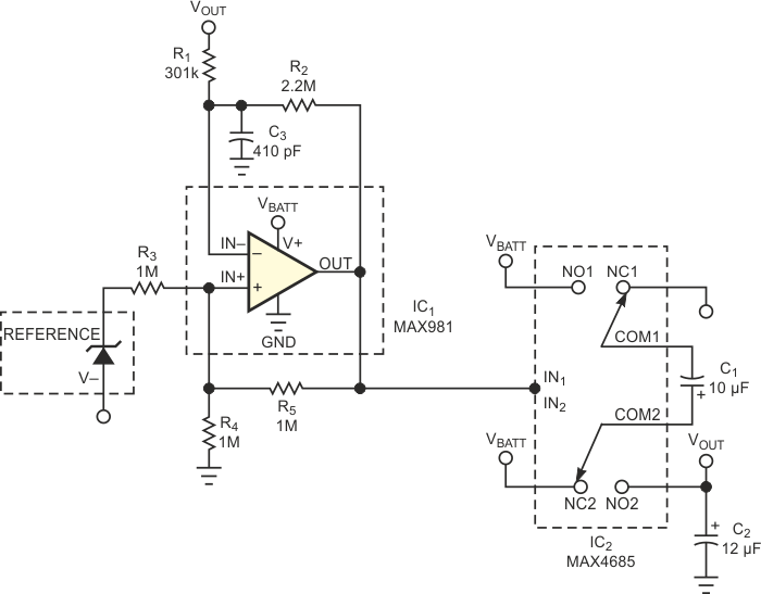
| Figure 1. | This charge-pump circuit uses analog switches to achieve ultralow quiescent current. | |
Charge pumps use an ac-coupling technique to transfer energy from a transfer capacitor to a storage capacitor. The transfer capacitor first charges via analog switches to the level of VBATT, and then other analog switches transfer the energy to a storage capacitor tied to VOUT. The transfer capacitor then charges again, and the cycle repeats. With ideal analog switches exhibiting zero loss, the VOUT level equals two times VBATT. As expected, however, the analog switches’ finite on-resistance produces an output level that drops in proportion to the load current. The basic regulated charge pump in Figure 1 includes an oscillator, several analog switches, a voltage reference, and a comparator. The comparator serves as a voltage monitor and an oscillator. When the circuit is in regulation, the comparator output is low, which closes the NC (normally closed) switches and allows C1 to charge to VBATT. When the voltage at VOUT dips below the output-regulation threshold – 3.3 V in this case – the comparator output goes high. The NO (normally open) switches close, transferring C1’s charge to C2. This cycle repeats until VOUT regains regulation.
Resistors R3 to R5 provide the hysteresis necessary for oscillation. Their value, 1 MΩ, creates a notable level of hysteresis and minimizes VBATT loading. As the comparator output changes state, feedback resistor R5 creates hysteresis by moving the threshold you apply to the comparator’s positive input. For the resistor values shown, reference value nominal for IC1 (1.182 V), and VBATT = 3 V, the VIN+ threshold swings between approximate values of VIN+(LOW) = 0.39 V and VIN+(HIGH) = 1.39 V. When the circuit is in regulation, VIN– slightly exceeds VIN+, the comparator output is low, the R1-R2 divider senses the voltage at VOUT, and the threshold at VIN+ is low (0.39 V). With VIN+ at 0.39 V, you can calculate the R1 and R2 values from the equation:
The resistance of R1 + R2 should be greater than 1 MΩ to minimize VBATT loading. If VOUT =3.3 V and R2 is 2.2 MΩ, R1 calculates to 301 kΩ. Capacitor C3 connects to the comparator’s IN– input. Along with R1 and R2, C3 sets the oscillation frequency according to the following simplified relationships:
and
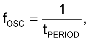
where tPERIOD = tLOW + tHIGH.
To maximize efficiency and reduce the effects of comparator slew rate, you should set a relatively low frequency. Choosing C3 = 470 pF yields the following: tLOW = 178 µsec, and tHIGH =68 µsec; thus, fOSC = 4 kHz.
Select the values of C1 and C2 to achieve the desired load current and ripple. For this application (ILOAD =10 mA), C1 =10 µF. To calculate the value of C2, make an approximation based on the desired ripple voltage:
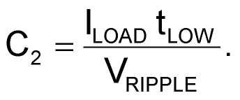
With ILOAD =10 mA and VRIPPLE =150 mV, C2 =12 µF.
With these component values, the circuit draws a maximum quiescent current of 6.9 µA and offers a considerable improvement over off-the-shelf charge pumps. You can further lower the quiescent current by increasing the resistor values, but that effect is minimal because IC2’s maximum quiescent current of 3.8 µA dominates the total. This circuit lets you implement an ultralow-quiescent-current-regulated charge pump. Until off-the-shelf options are available, it provides an alternative for designers seeking to implement a low-cost design without the use of inductors.