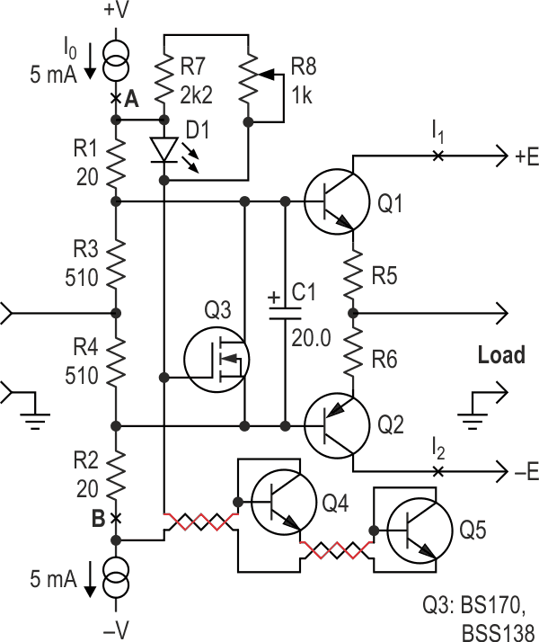
A widely-used push-pull configuration of an AB class amplifier is shown in Figure 1, but it needs some improvements.
 |
||
| Figure 1. | This configuration of an AB class amplifier have some improvements. | |
First of all, let’s take a look how its thermal compensation works. Q1 and Q2 represent shortcuts for the output transistors because usually these output devices are Darlington or complementary pairs. The bias voltage for Q1 and Q2 adds up from the zener (D1) voltage and the VBE drops of the Q4 and Q5 transistors, which are temperature-dependent. Normally Q4 and Q5 are located on the same heatsink(s) as transistors Q1 and Q2.
Usually the value of VBE (Uk in our context) is about 0.8 V (1.8-2.5 V if a Darlington configuration is used).
The quiescent currents through transistors Q1 and Q2 are:
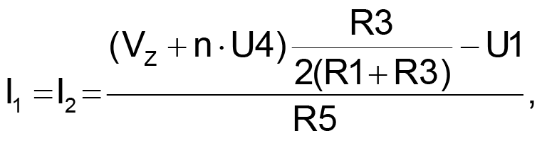
where n is the number of transistors in the compensation chain (2 transistors, Q4 and Q5, in Figure 1) and Uk, where k=1, 2, 3, 4 is VBE of transistor Qk.
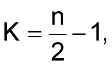
Let K = R1/R3, then:
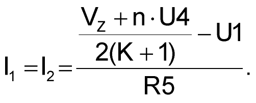
Taking a derivative:
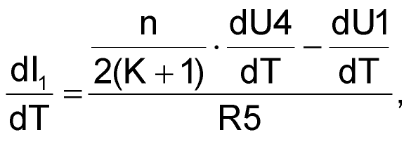
where the derivative dUk/dT stands for the thermal dependence of VBE of transistor Qk, k=1,2,3,4.
So, for instance, if the UBE thermal dependences of transistors U1 and U4 are close, then an optimum condition follows:
which is more or less evident, but we had to get it formally.
The compensation can be increased by connecting more transistors in series: two serially connected transistors Q4 and Q5 are used instead of only one. So the voltage change can be doubled. This also helps when the transistors Q1 and Q2 do not share a common heatsink. Then, Q4 (Q5) could be placed on the same heatsink with Q1 (Q2) to control the temperature.
The advantage of a Zener diode over a resistor in this design is for lower attenuation in the thermal feedback, hence a more precise compensation can be achieved. TL431 is preferable to an ordinary Zener diode since the TL431 has far lower dynamic resistance and allows for a lower working current.
All such kinds of thermal compensation have the same vulnerability: since the thermal sensor (Q4, Q5 in our case) needs to be placed on the output transistors’ heatsinks (i.e. remotely and not on the common PCB), some connecting wiring, with or without a socket, is almost unavoidable (note the wires to Q4 and Q5 in Figure 1).
If the chain of the thermal sensor (that chain is D1, Q4, Q5 in our case) is broken due to a bad contact in the socket or simply a break in a wire, this will inevitably generate a large and uncontrollable through current in the transistors Q1 and Q2. These transistors can be destroyed by this current and the corresponding thermal runaway will occur.
The Q4/Q5 pair-selected, high quality complementary power transistors may be rather pricey, but the endangered load can be much more expensive!
Moreover, a circuit of this kind can include a potentiometer to regulate the quiescent current, which makes such a circuit vulnerable to the quality of the pot. Something should be provided to prevent that kind of disaster.
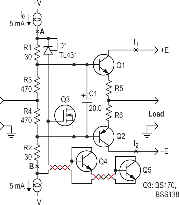
The circuit in Figure 2 can solve all these issues. It protects the expensive output transistors and the load from a large uncontrollable through current.
 |
||
| Figure 2. | This circuit protects the expensive output transistors and the load from a large uncontrollable through current. |
|
Here is how the protection works: the transistor Q3 controls the integrity of the chain D1, Q4, Q5. If the chain is open, the voltage on the gate of Q3 goes high, opening it and reducing the base bias of Q1 and Q2 to almost zero. This ensures very low quiescent currents I1 and I2, if the integrity is broken, as mentioned above.
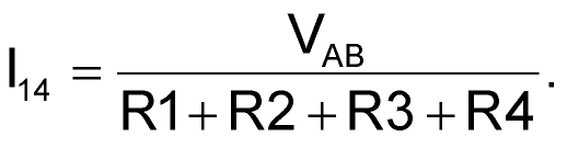
To calculate the components, let’s consider the maximum gate threshold voltage of Q3 for which this FET is open (off); we designate this value as VGS_O: VGS_O = 0.8 V (for BS170 and BSS138).
During normal operation, while the chain D1, Q4, Q5 isn’t broken, the transistor Q3 is open (off) and the voltage between points A and B is determined by the chain D1, Q4, Q5:

where, as above, U4 stands for VBE of Q4.
This can be true if:
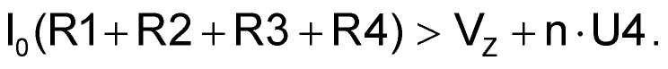
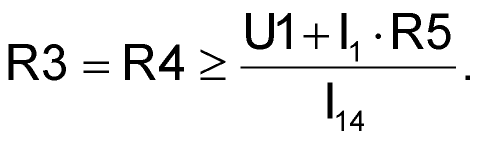
The current through R1, R2, R3, R4 is:
Suppose we do know the current I0; its value can be determined not only by the inequality above, but knowing the output power, the gain of the output transistors Q1/Q2, the frequency range, and the parasitic capacitance of the circuit.
Now the difference i0 – i14 should not be less than the minimum tolerant current of the Zener diode:
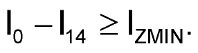
(This value can be found in the Datasheet, 1 mA for a TL431.)
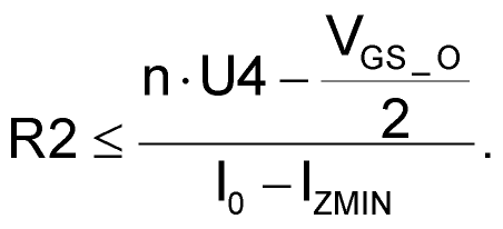
Then, for R2:
To be sure the transistor is open (off), let’s take only half of VGS_O:
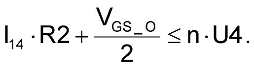
The values of R3 (R4) together with the thermal feedback chain (Q4, Q5, D1) should provide the necessary bias for Q1 (Q2):
Now let’s study what happens when the chain D1, Q4, Q5 is broken.
We designate VGS_C as the minimum value of VGS when Q3 is closed (on).
Then we have for VZ:
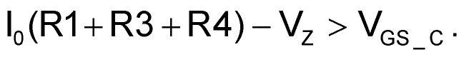
So we have for VZ:
The circuit in Figure 2 uses a green LED instead of a Zener diode. The advantages of this circuit are:
The LED indicates the integrity of the chain D1, Q4, Q5.
The current through the LED can be far less than through a Zener or a TL431.
A green LED is used here because it has the most appropriate drop voltage (about 2.2 V). Note: the drop depends on manufacturing technology and may be more than 3 V for some types of green LEDs, so be warned.
With the help of the chain R7, R8, we can control the through current I1 (I2). The chain will also be helpful for the case of a broken LED, limiting the voltage between A and B and the through current I1 (I2).
The capacitor C1 ensures zero quiescent current through transistors Q1 and Q2 during the circuit power-on. It also removes the AC difference on the bases of Q1 and Q2, eliminating the possible source of distortions.
Note the resistor pairs R1 and R2, R3 and R4 have the same value. This symmetry decreases the total harmonic distortion (THD) of the output stage (Reference 1).