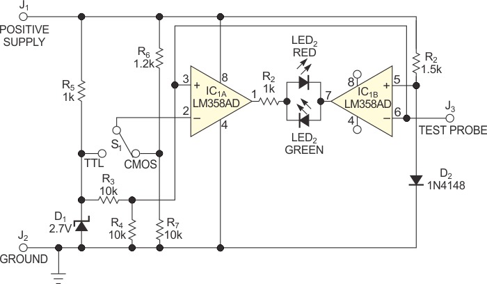
The circuit in Figure 1 uses the LM358 dual op amp running as a comparator, plus a few other inexpensive components, to make a TTL (transistor- transistor-logic)/CMOS-logic probe. The circuit gets its power from the circuit under test, which lets it work with TTL or CMOS logic. The IC1A and IC1B op amps come in an LM358 package. Switch S1 selects the TTL or the CMOS mode of operation. The green LED shows logic low, and the red LED shows logic high.
 |
||
| Figure 1. | Two comparators and some voltage dividers determine the status of a TTL or a CMOS-logic signal. | |
The noninverting input of IC1A and the inverting input of IC1B connect to the test probe. The circuit uses 90% of the power-supply voltage as CMOS-logic high and 2.7 V as TTL high. It uses 0.7 V as logic low for both TTL and CMOS because their logic-low levels approach 0.7 V. Voltage divider R3/R4 divides voltage from 2.7 V zener diode D1, providing 1.35 V at IC1A’s noninverting input and IC1B’s inverting input. Diode D2 is forward- biased, and the 0.7 V voltage across D2 becomes the lower limit, which represents logic low. You set this voltage on the noninverting input of IC1B.
In TTL mode, the voltage at the inverting input of IC1A is 2 V. In CMOS mode, the voltage at the inverting input of IC1A is nearly 90% of the input voltage through voltage divider R6/R7. When the probe is in its high-impedance state in either CMOS or the TTL mode, IC1A’s inverting input voltage is greater than its 1.35 V noninverting input voltage. IC1A’s output is low. IC1B’s 1.35 V inverting input voltage is greater than its 0.7 V noninverting input voltage. The output of IC1B is also low, and both LEDs are off.
In TTL mode, when measuring logic high, IC1A’s 2.7 V inverting input voltage is less than its noninverting input voltage, which is the probe voltage. IC1A’s output is high. IC1B’s inverting input voltage, which is the probe voltage, is greater than its 0.7 V noninverting input voltage. IC1B’s output is, therefore, low. The red LED turns on, indicating logic high. When measuring logic low, IC1A’s 2.7 V inverting input voltage is greater than the voltage at its noninverting input, which is the probe voltage. Thus, IC1A’s output is low. IC1B’s inverting input voltage, which is the probe voltage, is greater than its 0.7 V noninverting input voltage. Thus, IC1B’s output is high. The green LED turns on, indicating a logic low.
In CMOS mode, when measuring logic high, IC1A’s inverting input voltage, which is 90% of the supply voltage, is greater than the voltage at its noninverting input. The output is thus high. IC1B’s inverting input voltage, which is the probe voltage, exceeds that of its 0.7 V noninverting input voltage, and IC1B’s output is low. The red LED turns on, indicating logic high.
When measuring logic low, IC1A’s inverting input voltage, which is 90% of the supply voltage, exceeds the voltage at its noninverting input. IC1A’s output is low, and IC1B’s output is high because its inverting input voltage is higher than 0.7 V at its noninverting input voltage. The green LED turns on, indicating logic low. When the probe’s pin is pulsing, both LEDs alternately turn on and off at the pulse frequency.