Digital-system designs require you to consider many core voltages. Memory operates at 1.8 V, I2C and FPGA devices operate at 3.3 V, microcontrollers operate at 5 V, and charge-coupled-device image sensors operate at –9 to 8 V. Clocks for each device must suit their operating voltages.
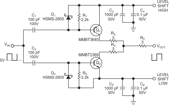
You can use the level-shift circuit in Figure 1 to adjust an input clock signal to the proper logic-high and logic-low voltage levels, including negative voltages. This property is handy for devices that need a negative voltage, such as a charge-coupled-device sensor. Although the circuit’s output clock is 180°-inverted relative to the input clock, that inversion does not affect the function of the device.
 |
||
| Figure 1. | This simple and fast level-shift circuit can adjust an input clock to both positive and negative voltage levels. |
|
The level-shift circuit comprises fast-switching transistors Q1 and Q2. The user chooses level-shift high and level-shift low, which are dc-bias voltages and which connect to the transistor emitters, to match the desired output high- and low-logic levels. C1, R1, D1,C2, R2, and D2 keep the base voltages of Q1 and Q2 close to that of their emitters.
Because memory and charge-coupled-device sensors usually have high-frequency clocks, you can choose C1 and C2 to prevent low-frequency-noise pass-through. The circuit in Figure 1 uses a 20-MHz signal for measurements (Table 1) and thus uses a value of 100 pF for C1 and C2. When the input voltage’s clock is low, Q1 turns on and Q2 turns off, driving the output voltage’s clock to the level shift’s high potential. When the input voltage’s clock is high, Q1 turns off and Q2 turns on, driving the output voltage’s clock to the level shift’s low potential, even when that potential is negative relative to ground.
| Table 1 | Input and output clocks | |||||||||||||||
|
||||||||||||||||
Because of the circuit’s high switching speeds, keep component leads as short as possible to minimize inductance. This caveat is especially true for C3 through C6’s leads to their respective transistor emitters and to the ground plane or the output ground return.