Abstract
This application report describes an alternative use of the TLC555-Q1 device as a charge pump. The square-wave output switching between the supply voltage and GND with few additional capacitors and diodes makes the device suitable for generating a positive or negative voltage multiplier. Using the TLC555-Q1 device as a charge pump is a cheap and easy solution for doubling, tripling, or inverting the supply voltage.
A charge pump can be used in automotive applications requiring reverse battery protection. A diode can also be used for battery protection; however, it causes a voltage drop and lowers efficiency. The charge pump is also capable of driving a MOSFET transistor with low drain-to-source on resistance.
Block Diagram Description
This device uses two window comparators, an RS flip-flop, an open-drain MOSFET, and a totem-pole output stage (Figure 1). The device also has a RESET pin for enabling and disabling the output. The supply voltage range of 2 V to 15 V enables the devices to work in an automotive environment with a fully-charged 12-V battery and during cold cranking.
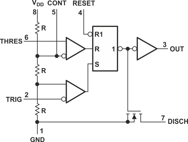 |
| Figure 1. |
Functional Block Diagram. |
Setup for Positive Charge Pump
The TLC555-Q1 device is configured as typical timer (Figure 2). The switching frequency and duty cycle is determined by the timing components R1, R2, and C5. The two diodes (D1, D2) and two ceramic capacitors (C3, C4) generate the positive charge pump 2VCC – 2VF. The D2 anode connected to VCC makes the charge pump voltage at VCC – 2VF when the TLC555-Q1 device is disabled. The charge pump can be at 0 V if the TLC555-Q1 device is disabled by connecting the D2 anode to the OUT pin (pin 3).
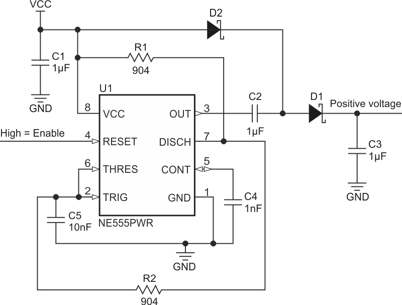 |
| Figure 2. |
Positive Charge-Pump Circuit. |
Power Up and Power Down
The device RESET pin can be used to enable and disable the charge pump according to Table 1.
| Table 1. |
Operation of Positive Charge Pump |
| RESET |
OUT pin 3 |
Charge Pump |
Doubler Level |
| High |
Switching |
ON |
2VCC – 2VF |
| Low |
Low |
OFF |
VCC – 2VF |
|
| |
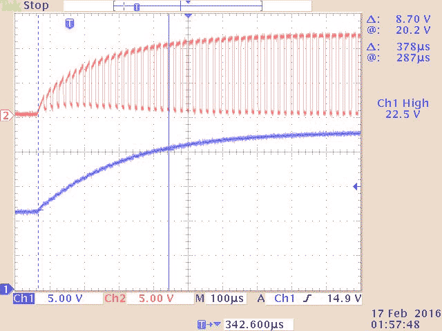 |
| Figure 3. |
Power-Up Timing – RESET Switching from Low to High. |
Figure 3 shows the power up timing by switching the RESET pin from low to high. Figure 4 shows the power down timing by switching the RESET pin from high to low.
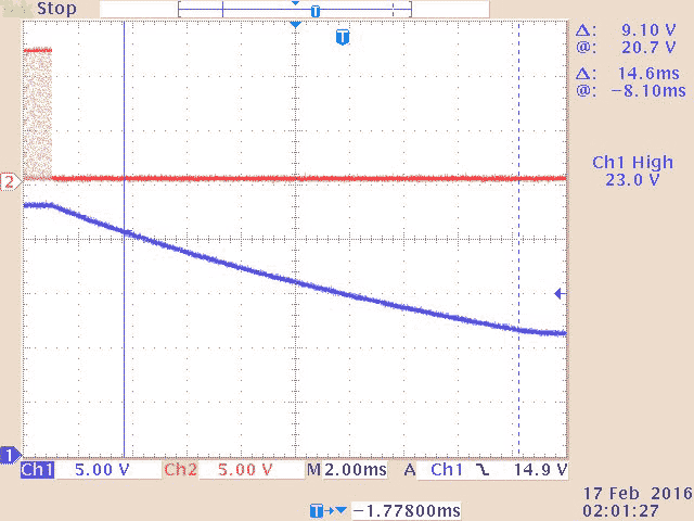 |
| Figure 4. |
Power-Down Timing – RESET Switching from High to Low. |
Characterization
The characterization of the doubler charge-pump circuit is at VCC = 12 V. The output is 2VCC – 2VF, where VF is the drop across a diode. Figure 5 shows the doubler charge pump versus the load current.
 |
| Figure 5. |
Charge-Pump Output Voltage versus Load Current. |
Setup for Negative Charge Pump
The TLC555-Q1 device is configured as typical timer (Figure 6). The switching frequency and duty cycle is determined by the timing components R1, R2 and C5. The 2 diodes (D1, D2) and 2 ceramic capacitors (C3, C4) generate the negative charge-pump inverter. The charge pump is at 0 V when the TLC555-Q1 device is disabled.
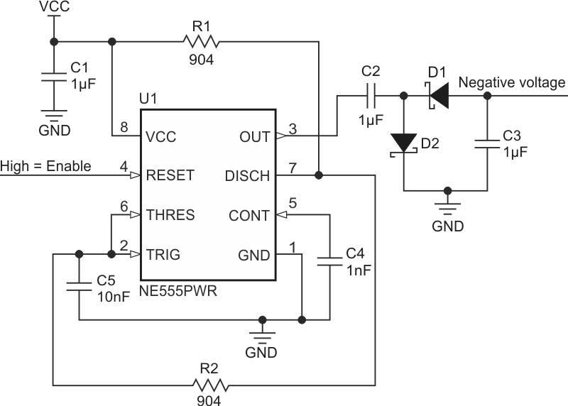 |
| Figure 6. |
Negative Charge Pump Circuit. |
Power Up and Power Down
The device RESET pin can be used to enable and disable the charge pump according to Table 2.
| Table 2. |
Operation of Negative Charge Pump |
| RESET |
OUT pin 3 |
Charge pump |
Inverting level |
| High |
Switching |
ON |
–VCC + 2VF |
| Low |
Low |
OFF |
0 |
|
| |
Figure 7 shows the power up timing by switching the RESET pin from low to high. Figure 8 shows the power down timing by switching the RESET pin from high to low.
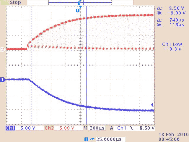 |
| Figure 7. |
Power-Up Timing – RESET Switching from Low to High. |
Characterization
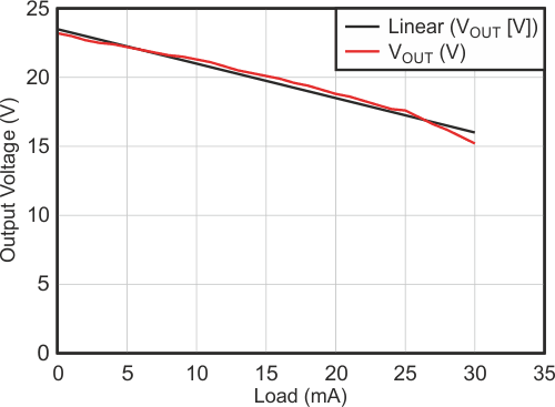
The characterization of the doubler charge-pump circuit is at VCC = 12 V. The output is –2VCC + 2VF, where VF is the drop across a diode. Figure 9 shows the negative doubler charge pump versus the load current.
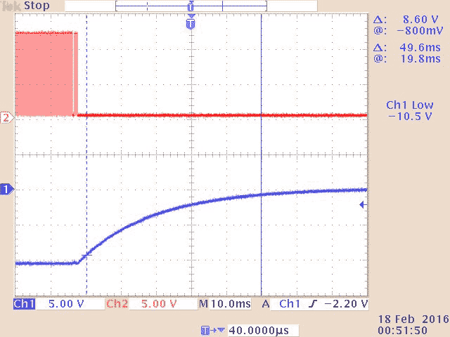 |
| Figure 8. |
Power-Down Timing – RESET Switching from High to Low. |
Summary
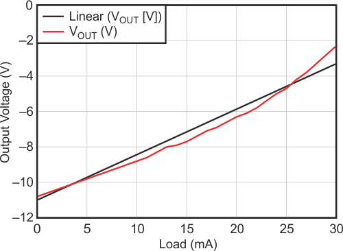 |
| Figure 9. |
Charge Pump Output Voltage versus Load Current. |
The TLC555-Q1 device can be configured in multiple charge-pump configurations with few external components. The device can be used as a cost-saving measure in many applications.
Materials on the topic
- Datasheet Texas Instruments TLC555-Q1