In power converters, pulse-drive circuits transmit the pulses a controller generates to the power transistor. Driver circuits must both transmit the controller's switching on/off signals with galvanic isolation and provide energy to turn the switch on and off and to maintain the required on or off state. The required energy increases with the power transistor's input capacitance, which also increases with the power that the transistor module manages. Thus, when the circuit requires high power, designers typically parallel the power transistors, increasing the input capacitance. When you need to operate IGBT (insulated-gate-bipolar-transistor) modules in parallel, it is best to share the gate drive because using different driver circuits introduces additional variation in turn-on and -off times and creates a possible imbalance between each power module.
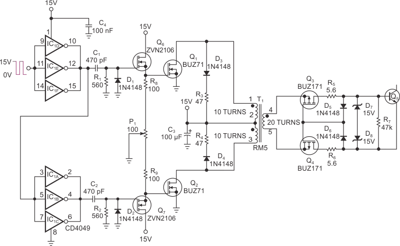
The basis of the circuit in Figure 1 is an earlier Design Idea (Reference 1). The operation of the circuits is basically the same as the one in the previous Design Idea, but this one can drive MOSFETs or IGBTs with input capacitances higher than 5 nF. This circuit provides full galvanic isolation and requires no floating power supplies; it can transmit duty cycles that approach 100%.
 |
|
| Figure 1. | This isolated pulse driver can transmit all duty cycles, even with high-power MOSFET/IGBT modules that have large input-gate capacitance. |
This circuit adds transistors Q6 and Q7 to the circuit in the previous Design Idea. Transistors Q1, Q2, Q3, and Q4 are now higher power because they can manage a larger current depending on the transistor they need to drive. Transistors Q1 and Q2 are BUZ71 units, Q3 and Q4 are BUZ171 devices, and Q6 and Q7 are ZVN2106s. The differentiator circuits, C1/R1 and C2/R2, generate 1-μsec-long pulses, and you do not apply them directly to the gates of the Q1 and Q2 transistors, as in Reference 1, but to transistors Q6 and Q7. Although the input capacitances of Q1 and Q2 are nearly 700 pF, the input capacitances of Q6 and Q7 are approximately 75 pF, ensuring that the narrow pulses will transmit properly.
During the rising edge of the drive-control signal, Q7 turns on, and its current starts charging the input capacitance of Q2 through the on-resistance of Q7. Because Q7's on-resistance is only a few ohms and no additional drain resistance exists, the charging process of Q2's input capacitance becomes fast, although its input capacitance is high.
As the gate voltage of Q2 increases, the gate-to-source voltage of Q7 decreases, and the transistor turns off. As a result, the narrow pulses that the differentiator circuit generates transmit to transistors Q7 and Q2 through coupling transformer T1 to transistor Q3, which charges Q5's gate-to-source input capacitance. The same process occurs with Q6, Q1, and Q4 during the falling edge of the drive-control signal to discharge Q5's gate-to-source input capacitance.
With potentiometer P1, you can control the discharge time of Q1 and Q2 and thus adjust the offset of the drive signal you apply to the power transistor. Because Q6/Q1 and Q7/Q2 transmit narrow pulses and have fast rising and falling edges, you can obtain a great duty-cycle variation even for high switching frequencies. You can control the duty cycle from 2 to 98% with a 20-kHz switching frequency. The circuit's compact design lets you mount it close to the power module, which minimizes parasitic elements.
 |
|
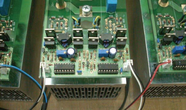
| Figure 2. | An isolated FET pulse driver in a 10-kW, three-phase inverter for grid injection requires few components and has galvanic isolation. |
Figure 2 shows the driver prototype for a 10-kW/20-kHz three-phase power inverter for grid injection. The circuit uses SKM75GB128 power transistors from Semikron. The transistors have a measured input capacitance higher than 15 nF. In this situation, the total current consumption of the FET pulse driver is lower than 30 mA.