The inverters in a CMOS CD4069 can be used for both analog as well as digital applications. This Design Idea illustrates this by using all six inverters in a 4069 package to make a closed loop, duty-cycle-based capacitance meter with a full scale deflection below one picofarad.
The inverters exhibit stable output with a direct feedback connection: When the input of one gate is directly connected to the output, the resulting output is around VT, the threshold voltage. If a resistor R is connected between the input and ground, a current equal to ~VT/R flows, as shown in Figure 1b. Its magnitude remains fairly constant, even when a resistor – small compared to R – is introduced in the feedback loop. The voltage window ΔVT around VT that changes the gate's output from logic-0 to logic-1 is very small compared to VT itself. This means the voltage across R would remain within VT ± ΔVT/2, yielding an approximately constant current through it (since the output voltage can have a value up to VDD, up to VDD – VT can be dropped across the feedback resistor). The feedback loop is thus a source of constant current.
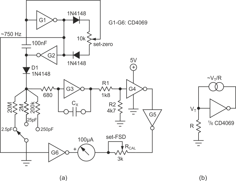
By having a capacitor within this loop, one can charge it at a constant rate, giving rise to a linearly rising voltage ramp. This technique is applied in the circuit of Figure 1a to build a picofarad full scale deflection (FSD) capacitance meter. It consists of a two-gate astable (G1, G2), a single-gate voltage ramp generator (G3) whose slope depends on the value of the test capacitor CX, a single-gate voltage level detector (G4), and two buffers (G5, G6) which drive the meter through the calibrating resistor RCAL.
The reading due to stray capacitance can be nulled by adjusting the duty cycle of the astable with the 10 kΩ set-zero pot. The astable drives the ramp generator through isolating diode D1, which serves to rapidly discharge CX, but which allows charging through the ramp resistor (20 MΩ/ 2 MΩ/ 200 kΩ) alone. A reverse-biased diode has an effective resistance on the order of 109 Ω, and hence is much larger than even the 20 MΩ resistor.
 |
|
| Figure 1. | 2.5 pF-250 pF FSD capacitance meter using all six inverter gates of a CD4069 (a). A single-gate constant current source (b). |
The complementary output of the astable drives G6, whose output drives one of the terminals of the meter. Gate G4 acts as a level detector for the ramp through the divider network R1/R2 (resistance values can be increased if desired). The output of G4 is buffered by G5, whose output drives another terminal of the meter. The ramp effectively introduces a delay in the falling ouput of the astable, directly proportional to the value of CX. This delay produces a voltage difference across the meter for part of the cycle, resulting in a display of the value of CX. An RC filter may be needed if driving a digital meter.
The high impedance of the CMOS inputs is another essential feature that makes this design work, allowing large resistors like 20 MΩ or more across its input. This simple circuit uses only a single 4069 inverter chip to make a complete, reliable capacitance meter.
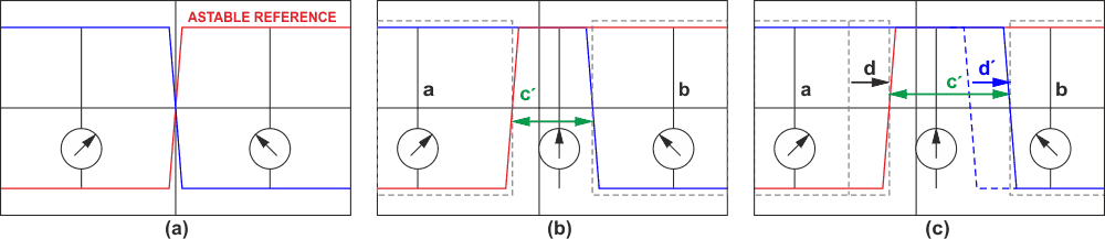
The operation of the scheme is explained by the waveforms in Figure 2.
 |
|
| Figure 2. | Diagrams explaining the operation of the circuit in Figure 1. Blue color: the input signal of G5 gate, red color: the input signal of G6 gate. |
Figure 2a shows 50% duty cycle signal when applied to a meter through two gates, 180° out of phase. The average difference is zero, hence the meter shows no deflection.
Figure 2b shows stray capacitance compensated waveform from the astable, where a and b phases produce equal and opposite deflection in the meter causing a net null deflection. However the delay along the ramp line causes one of the signals to have an offset for a duration (c'- null phase). During this null phase (c') the net potential difference across the meter is zero so it contributes no deflection. Overall during the entire period, the meter has net zero algebraic deflection. It should be noted that stray capacitance compensation is provided by adjusting the astable duty cycle which is represented by the red waveform.
Figure 2b shows waveforms across the meter when an external capacitor to be measured CX is introduced in the ramp circuit. This causes additional delay causing asymmetric deflection moments in the meter, the phase a now lasts for a relatively longer period compared to phase b by an amount d' proportional to the value of the capacitor CX. So for one astable period (T) the residual algebraic deflection in the meter now is for duration d(=d'). The average deflection seen in the meter now depends on d/T which in turn measures test capacitor's value.
 |
|
| Figure 3. | Implementation of PWM using two inverters. |
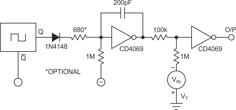
Another application of the constant current source integrator is to realize PWM using only two gates (Figure 3). VIN introduces a voltage across the 100 kΩ resistor which the ramp has to overcome in order to switch the output gate. If needed, VT bias can be obtained using another gate with output connected to input.