CMOS devices have large input impedance with input currents on the order of 0.01 nA. Adding feedback circuitry can result in a latch-like device that can be used to store bits, and also operate in a more analog mode as shown in this Design Idea, which pinpoints the location of a break in a wire.
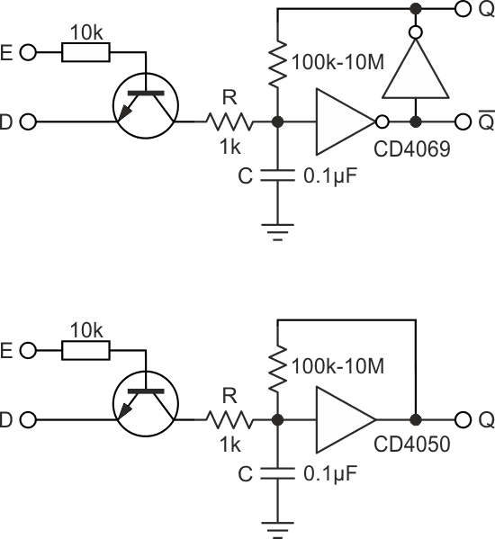
First let’s look at the use of CMOS gates as memory devices. Figure 1 shows a one-bit transparent latch. A single CD4069 hex inverter can make a 3-bit latch, or if one uses a CD4050 hex buffer one can have a 6-bit latch. In the case of inverters, a pair of gates form a memory cell. One gate feeds back the inverted output from the other through a large resistor.
 |
|
| Figure 1. | Transparent latch using ordinary CMOS gates. Data in is “D” and enable is “E”. |
A small capacitor is also included at the input which provides noise immunity (either supply or at the input). It also helps to set up timing constraints for the input signals. A transistor is used to latch data into the memory cell. The emitter of the NPN transistor is used to supply the data, and its base terminal is used to control its transmission to the input of the cell. Data is applied to D, and a short positive pulse is applied to E. In a time determined by the RC time constant, this data is copied into the memory cell. Inverter gate based memory cells can provide both non-inverted and inverted outputs while non-inverting gate provides only non-inverted output. The feedback resistor can also be a reverse biased diode, as the input impedance of the gates is very high. A reverse biased diode conducts current on the order of 1 nA, which is still two orders of magnitude higher than the input current requirement of the CMOS gate.
In a bundle of wire with a break somewhere along it, though it is simple to tell whether or not there is a break, it is difficult to pinpoint its location. Using the above discussed memory cell, we shall explore a way of detecting such a break.
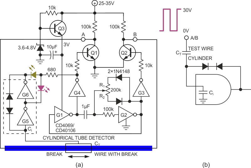
In Figure 2a, the broken wire forms a capacitance with a detector cylinder of length 1-3 cm through which the wire passes, and charges the input capacitance (CI ~10 pF) of G5. The cylinder/wire configuration can have a capacitance on the order of a few pF or less. Hence, to store the required amount of charge on G5’s input, a large voltage is required. The opposite ends of the broken wire are connected to out-of-phase square waves of ~30 V amplitude. Schematically we have a ~1 pF and ~10 pF capacitor series combination being charged by a potential difference of 30 V (Figure 2b). To toggle the gate, the voltage on its input capacitance CI should vary on the order of VT, its input logic threshold voltage. The gates operate at a voltage of only 3 V, even though the supply is 25 - 35 V. A 3 V supply to CD4069/ 40106 implies a VT of roughly 1.5 V. Even though both the capacitors have the same charge, their voltages are different by a factor of 10 – if the gate input capacitor CI is charged to ~1.5 V, the wire-cylinder capacitor CT is charged to ~15 V. Thus, a supply of 25-35 V is a good choice to generate the square wave signal applied to the two ends of the test wire.
 |
|
| Figure 2. | Schematic diagram of wire break detector using CMOS memory cell (shown in broken box). If using the CD40106, only one gate is needed for the oscillator (Schmitt inputs). An additional gate can be put in series with the memory cell G5 and G6 to form a completely separate LED driver. One can directly use a dual color LED if desired as the LEDs can be reversed in orientation simultaneously. Use of bright LEDs and a supply of at least 30 V is recommended. It is also possible to use a resistor divider network at the base of Q3 to obtain the 3 V supply. When the tube passes over the break, there is a flip in the glow of the LEDs. It should be cautioned that some versions of the CD4069 might not function properly as an astable due to a low value of VT. |
The square wave is generated using gates G1-G4. The outputs from G3 & G4 control Q1 & Q2 in opposite phase. Gates G5 & G6 form the memory cell which stores the logic state arriving at the input. The LEDs indicate the memory content at the chosen phase of the astable (here, the output of G4). When the tube passes across the break, the LEDs change state.
 |
|
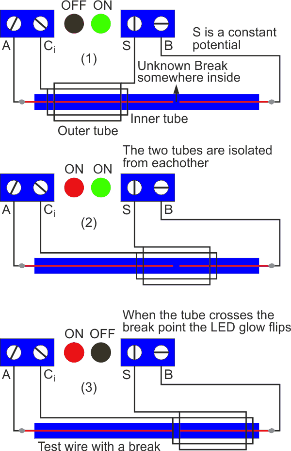
| Figure 3. | This shows how the LEDs respond to sleeve position. |
 |
|
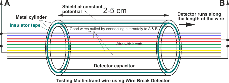
| Figure 4. | Suggested connection for a multiconductor cable. |