When a design needs auxiliary voltage rails and the associated current loads are modest, capacitor pump voltage multipliers are often the simplest, cheapest, and most efficient way to make them.
The simplest of these is the diode pump voltage doubler. It consists of just two diodes and two capacitors but has the inherent disadvantages of needing a separately sourced square wave for drive and of producing an output voltage that’s at least two diode drops less than twice the supply rail. Active switching (typically with CMOS FETs) is required to avoid this inefficiency and accurately double the supply.
CMOS voltage doubler chips are available off the shelf. An example is the Maxim MAX1682. It serves well in applications where the current load isn’t too heavy, but it (and similar devices) isn’t particularly cheap. The 1682 costs nearly $4 in singles, creating the temptation to see if we can do better, considering that generic CMOS switch chips (like the 74AC14) can be had in singles for 50 cents.
A plan to do so begins with Figure 1, showing a simplified sketch of a CMOS logic inverter.
 |
|
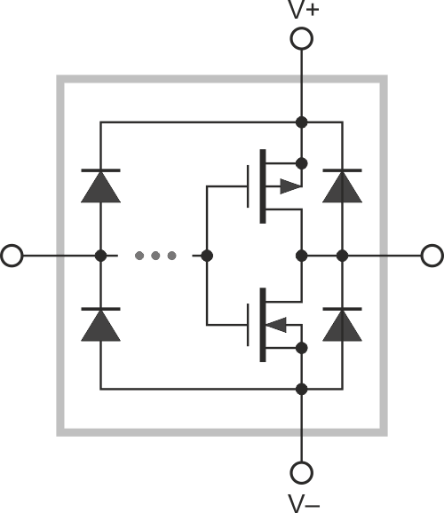
| Figure 1. | Simplified schema of typical basic CMOS gate I/O circuitry showing clamping diodes and complementary FET switch pair. |
Notice the input and output clamping diodes. These are put there by the fabricator to protect the chip from ESD damage, but a diode is a diode and can therefore perform other useful functions, too. Similarly, the P-channel FET pair was intended to connect the V+ rail to the output pin when outputting a logic ONE, and the N-channel for connection to V- to pin for a ZERO. But CMOS FETs will willingly conduct current in either direction. Thus, current running from pin to rail works equally well as from rail to pin.
Figure 2 shows how these basic facts relate to charge pumping and voltage multiplication.
 |
|
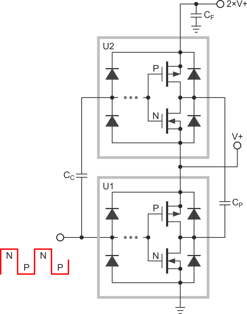
| Figure 2. | Simplified voltage doubler, showing driver device (U1), commutation device (U2), and coupling (CC), pump (CP), and filter (CF) capacitors. |
Imagine two inverters interconnected as shown in Figure 2 with a square-wave control signal coupled directly to U1’s input and through DC blocking cap CC to U2 with U2’s input clamps providing DC restoration.
 |
|
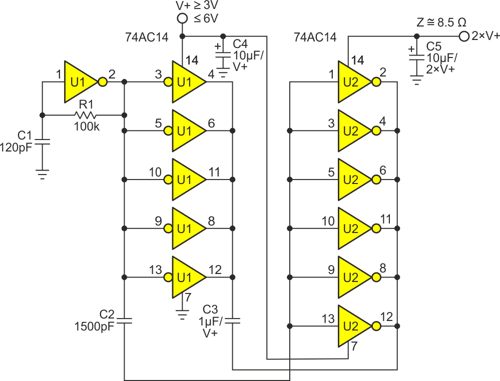
| Figure 3. | Complete voltage doubler: 100 kHz pump clock set by R1C1, Schmidt trigger, driver (U1), and commutator (U2). |
Consider the ONE half cycle of the square-wave. Both U1 and U2 N-channel FETs will turn on, connecting the U2 end of CP to V+ and the U1 end to ground, charging CP to V+. Note the reversed polarity of current flow from U2’s output pin due to CP driving the pin negative.
Now consider what happens when the control signal reverses to ZERO.
The P FETs will turn ON while the N FETs turn OFF. This forces the charge previously accepted by CC to be dumped to CF through U2’s output and V+ pin, thus completing a charge-pumping cycle that delivers a quantum of positive charge to be deposited on CF. Note reversed current flow through U2 occurs again. The cycle repeats with the next alternation of the control signal, and so on, etc., etc.
During startup, until sufficient voltage accumulates on CF for normal operation of U2’s internal circuitry and FET gate drive, U2 clamp diodes serve to rectify the CP drive signal and begin the charging of CF until the FETs can take over.
So much for theory. Translation of Figure 2 into a complete voltage doubler is shown in Figure 3.
A 100 kHz pump clock is output on pin 2 of 74AC14 Schmidt trigger U1. This signal is routed to the five remaining gates of U1 and (via coupling cap C2) the six gates of U2. Positive charge transfer occurs through C3 into U2 and from there accumulates on filter cap C5.
Even though Schmidt hysteresis isn’t really needed for U2, another AC14 was chosen for it in pursuit of matched switching delay times, thus improving efficiency-promoting synchronicity of charge transfer.
Some performance spec’s (V+ = 5 V) are:
- Impedance of 10 V output: 8.5 Ω
- Maximum continuous load: 50 mA
- Efficiency at 50 mA load: 92%
- Efficiency at 25 mA load: 95%
- Unloaded power consumption: 440 µW
- Startup time < 1 millisecond
 |
|
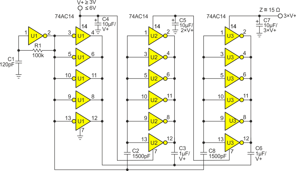
| Figure 4. | Adding four inexpensive parts suffices to triple the supply voltage. |
So, what happens if merely doubling V+ isn’t enough? As Figure 4 illustrates, this design can be easily cascaded to make an efficient voltage tripler. Extension to even higher multiples is also possible.