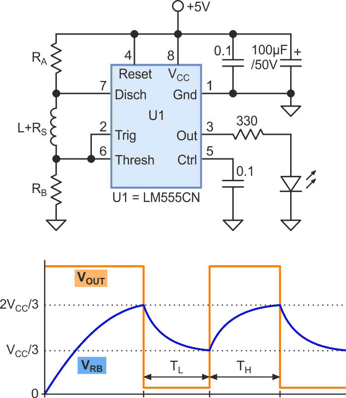
The 555 multivibrator circuit has become a default choice of many hobbyists and even professionals in the past 50 years. Its pair of equations for frequency and duty cycle easily gives capacitor-resistor combinations which satisfy the required output. But there could be situations when using inductor-resistor values instead would be a better solution. An example is a high-temperature environment which can shorten the useful life of electrolytic capacitors. In that case, the circuit in Figure 1 is worth considering.
At start-up, the voltage at pin 2 (VRB) is zero and the output (VOUT) at pin 3 is high. During this time the LED is on and the discharge transistor (pin 7) is open. The inductor current increases exponentially until VRB reaches 2VCC/3. This is sensed by the threshold terminal (pin 6) which causes VOUT to go low. The discharge transistor turns on and the LED turns off.
 |
|
| Figure 1. | A 555 multivibrator circuit that uses inductor-resistor values. |
Pin 7-to-ground effectively provides a low-resistance path (RON) which causes the inductor current and VRB to gradually decrease towards zero. When pin 2 senses that VRB has fallen below VCC/3, VOUT goes high again, the LED turns on, and pin 7 reverts to its open state.
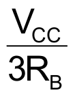
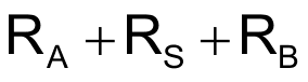
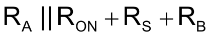
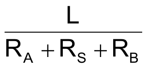
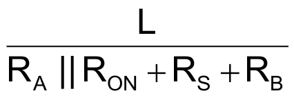
To calculate the ensuing values of high time (TH) and low time (TL) of VOUT, we can use Equation 1 which comes from the step-response analysis of an R-L circuit. It gives the duration for charging (or discharging) current to change from an initial to a final value:
 |
(1) |
The symbols in Equation 1 are defined in Table 1.
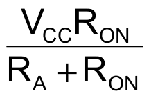
In addition, RS is the inductor’s DC resistance which is not negligible when the quality factor (Q) is low. There is also according to Rogers [Reference 1]
Applying these in the effective circuit during each interval, the symbols take up particular values as shown in the columns for TH and TL of Table 1. It is beneficial to do all the calculations on a spreadsheet, especially when we want to find out how sensitive the output is to the tolerances of the components.
|
||||||||||||||||||||||||||||
|
||||||||||||||||||||||||||||
|
||||||||||||||||||||||||||||


 |
|
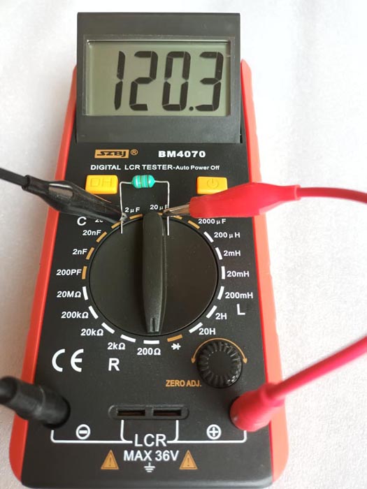
| Figure 2. | RS of the inductor. |
To test these ideas, I picked the components listed in Table 2 and used an LCR meter to measure their actual characteristics (Figure 2). I plugged the values into the spreadsheet to predict TH, TL, and other output characteristics. The results of these calculations are listed in Table 3.
 |
|
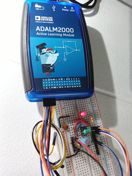
| Figure 3а. | The experimental set-up. |
 |
|
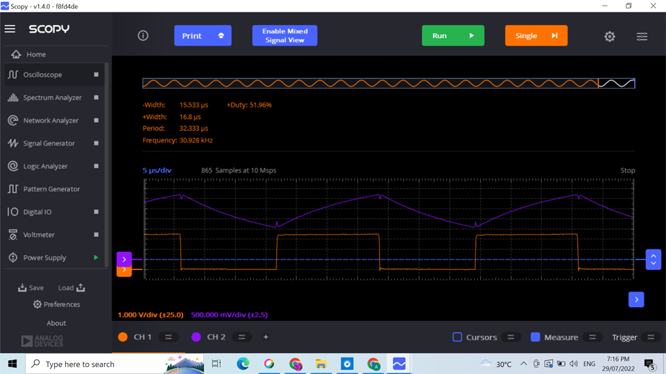
| Figure 3b. | Waveforms of VRB and VOUT, and measurements for VOUT. |
I used the ADALM2000 module (from Analog Devices) to power the experimental set-up (Figure 3a) and get the waveforms (Figure 3b) from pins 2 and 3 of the timer IC. The measurements show that Equation 1, in tandem with those of Table 2, closely models the behavior of the proposed circuit. There were droops and spikes noted for VRB during the transitions at pin 7, mostly due to the long power lines. These were mitigated by the pair of capacitors placed very close to pin 8.