Mechanical bounce often occurs while trying to measure current or resistance on experimental materials or from routine switch-contact action. It can be a problem if you are trying to preserve the bounce or noise phenomenon within the measurement system itself. Typically, such switch-bounce or similar noise is eliminated by using filtering or software delays that implement “guesses” on when the unknown disturbances may have subsided.
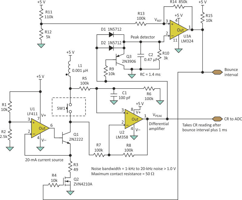
The circuit of Figure 1 allows analysis of noise or mechanical bounce within time intervals set by a simple peak detector with an associated comparator. Switch-contact resistance then can be read automatically through the differential amplifier by using the known current source (set here at 20 mA).
 |
|
| Figure 1. | The analog peak detector develops a “window” around the switch-bounce period, enabling measurement of contact resistance using a current source. |
The resultant signal can be digitized to measure bounce times. When the bounce has subsided, it allows very accurate contact-resistance measurements. This band-limited process requires no oscilloscope, time delays, or filtering. It also automatically quantifies the mechanical-noise activities.
This circuit will enable a contact-resistance measurement only when noise is not present at the output of differential amplifier U2, pin 1 (VPEAK). The switch bounce/noise amplitude will have to be larger than 1 V (peak), and the bounce/noise frequency must be greater than 1 kHz (period less than 1 ms).
When the sample switch is closed, potential noise could develop at the simple differential amplifier, which has gain of
An output greater than 1 V will be enough to overcome the threshold of peak-detector diodes D1 and D2 and, at the same time, turn off transistor Q3, which enables the RC-time constant of R10 and C2, currently set at 1.40 ms.
However, it can be set higher, which will enable slower-frequency components to influence the hysteresis comparator. The RC time constant must be longer than the desired noise transitions. (Note that the comparator is also designed to incorporate hysteresis.)
For the hysteresis detector to disable the current source, VPEAK from output of the differential amplifier must be greater than
Similarly, for the comparator to enable current-source readings, VPEAK must be below
In this example, peak-detector voltage VREF is set at 0.217 V.
Once the noise from the output of the amplifier drops below 1 V or the transitions become longer then the RC time constant set by R10 and C2, transistor Q3 will turn on, quickly disabling the RC time constant available for the detector and then the comparator will reset. Once the comparator is reset, it can then enable FET transistor Q2 to provide the contact-resistance reading without interference.
The current source is used to provide constant current through transistors Q1 and Q2, here set to 20 mA, via the 1-V/50-Ω pairing. The 1-V control is provided by the simple op-amp U1. (Be sure to include the on-resistance RDS(on) of the enable FET when setting up the current source.)
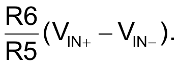
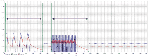
In the noise-capture event simulation, the blue trace is the voltage output of the differential amplifier, the red trace is the voltage developed by the output of the RC-peak detector network, and the green trace shows the action of the hysteresis detector (Fig. 2).
 |
|
| Figure 2. | The noise-capture event is characterized by the output of the differential amplifier (blue trace) the output of the RC-peak detector network (red) and the action of the hysteresis detector (green) here for a pair of noise bursts of different periods. |
The first noise-bounce burst is set at 1 kHz, 1.5 V. The second burst is at 20 kHz, at the same amplitude. The black arrows indicate a time interval representing switch bounce. Contact-resistance readings then can be enabled when the square pulses (green) are high. The contact resistance (the blue trace, when enabled) is close to 0.8 V, which indicates a resistance of 40 Ω.
 |
|
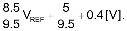
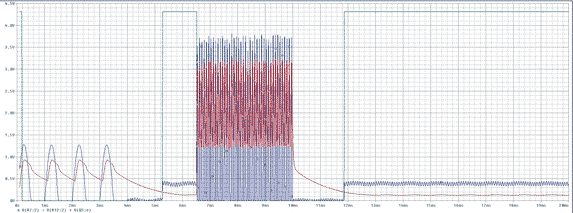
| Figure 3. | The noise bursts are set at 1.25 and 3.5 V, and the contact resistance is 0.4 V, indicating a resistance of 20 Ω. |
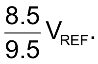
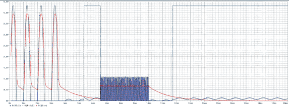
In Figure 3, the noise bursts are set at 1.25 and 3.5 V, and the contact resistance is 0.4 V, indicating a resistance of 20 Ω. Finally, in Figure 4, the noise bursts are 4.25 and 1.10 V, and the contact resistance is close to 0 V, which, of course, indicates a resistance of 0 Ω.
 |
|
| Figure 4. | The noise bursts are 4.25 and 1.10 V, and the contact resistance is close to 0 V, which indicates a resistance of 0 Ω. |